Energy Bands
Category : JEE Main & Advanced
This theory is based on the Pauli exclusion principle.
In isolated atom the valence electrons can exist only in one of the allowed orbitals each of a sharply defined energy called energy levels. But when two atoms are brought nearer to each other, there are alterations in energy levels and they spread in the form of bands.
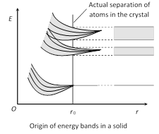
Energy bands are of following types
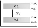
(1) Valence band : The energy band formed by a series of energy levels containing valence electrons is known as valence band. At 0 K, the electrons fills the energy levels in valence band starting from lowest one.
(i) This band is always filled with electrons.
(ii) This is the band of maximum energy.
(iii) Electrons are not capable of gaining energy from external electric field.
(iv) No flow of current due to electrons present in this band.
(v) The highest energy level which can be occupied by an electron in valence band at 0 K is called fermi level.
(2) Conduction band : The higher energy level band is called the conduction band.
(i) It is also called empty band of minimum energy.
(ii) This band is partially filled by the electrons.
(iii) In this band the electrons can gain energy from external electric field.
(iv) The electrons in the conduction band are called the free electrons. They are able to move any where within the volume of the solid.
(v) Current flows due to such electrons.
(3) Forbidden energy gap \[(\Delta {{E}_{g}})\] : Energy gap between conduction band and valence band \[\Delta {{E}_{g}}={{(C.B.)}_{\min }}-{{(V.B.)}_{\max }}\]
(i) No free electron is present in forbidden energy gap.
(ii) Width of forbidden energy gap depends upon the nature of substance.
(iii) As temperature increases \[(\uparrow )\], forbidden energy gap decreases \[(\downarrow )\] very slightly.
Types of solid
| Properties | Conductors | Insulators | Semiconductors |
| Electrical conductivity | \[{{10}^{2}}\] to 108 ?/m | \[{{10}^{8}}\,\mho /m\] | \[{{10}^{-5}}\] to \[{{10}^{0}}\,\mho /m\] |
| Resistivity | \[{{10}^{-2}}\] to \[{{10}^{-8}}\,\,\Omega -m\] (negligible) | \[{{10}^{8}}\,\,\Omega -m\] | \[{{10}^{5}}\] to \[{{10}^{0}}\,\,\Omega -m\] |
| Band structure |  |
 |
 |
| Energy gap \[({{E}_{g}})\] | Zero or very small | Very large; for diamond it is 6 eV | Ge \[\to \] 0.7 eV Si \[\to \] 1.1 eV GaAs \[\to \] 1.3 eV GaF2 \[\to \] 2.8 eV |
| Current carriers | Free electrons | - | Free electrons and holes |
| Condition of V.B. and C.B. at ordinary temperature | V.B. and C.B. are completely filled or C.B. is some what empty | V.B. - completely filled C.B. -completely unfilled | V.B. - somewhat empty C.B. - somewhat filled |
| Temperature co-efficient of resistance | Positive | Zero | Negative |
| Effect of temperature on conductivity | Decreases | - | Increases |
| Effect of temperature on resistance | Increases | - | Decreases |
| Examples | Cu, Ag, Au, Na, Pt, Hg etc. | Wood, plastic, mica, diamond, glass etc. | Ge, Si, Ga, As etc. |
| Electron density | \[{{10}^{29}}/{{m}^{3}}\] | - | \[Ge\tilde{\ }{{10}^{19}}/{{m}^{3}}\] \[Si\tilde{\ }{{10}^{16}}/{{m}^{3}}\] |


You need to login to perform this action.
You will be redirected in
3 sec

