0
question_answer1) Assertion : The logic gate NOT can be built using diode. Reason : The output voltage and the input voltage of the diode have 180° phase difference. [AIIMS 2005]
question_answer2) Assertion : The number of electrons in a P-type silicon semiconductor is less than the number of electrons in a pure silicon semiconductor at room temperature. Reason : It is due to law of mass action. [AIIMS 2005]
question_answer3) Assertion : In a common emitter transistor amplifier the input current is much less than the output current. Reason : The common emitter transistor amplifier has very high input impedance. [AIIMS 2005]
question_answer4) Assertion : A transistor amplifier in common emitter configuration has a low input impedence. Reason : The base to emitter region is forward biased. [AIIMS 2004]
question_answer5) Assertion : The resistivity of a semiconductor increases with temperature. Reason : The atoms of a semiconductor vibrate with larger amplitude at higher temperature there by increasing it's resistivity. [AIIMS 2003]
question_answer6) Assertion : If the temperature of a semiconductor is increased then it's resistance decreases. Reason : The energy gap between conduction band and valence band is very small [AIIMS 1997]
question_answer7) Assertion : The temperature coefficient of resistance is positive for metals and negative for P-type semiconductor. Reason : The effective charge carriers in metals are negatively charged whereas in P-type semiconductor they are positively charged. [AIIMS 1996]
question_answer8) Assertion : Electron has higher mobility than hole in a semiconductor. Reason : Mass of electron is less than the mass of hole.
question_answer9) Assertion : An N-type semiconductor has a large number of electrons but still it is electrically neutral. Reason : An N-type semiconductor is obtained by doping an intrinsic semiconductor with a pentavalent impurity.
question_answer10) Assertion : The crystalline solids have a sharp melting point. Reason : All the bonds between the atoms or molecules of a crystalline solids are equally strong, that they get broken at the same temperature.
question_answer11) Assertion : Silicon is preferred over germanium for making semiconductor devices. Reason : The energy gap for germanium is more than the energy gap of silicon.
question_answer12) Assertion : We can measure the potential barrier of a PN junction by putting a sensitive voltmeter across its terminals. Reason : The current through the PN junction is not same in forward and reversed bias.
question_answer13) Assertion : Semiconductors do not Obey's Ohm's law. Reason : Current is determined by the rate of flow of charge carriers.
question_answer14) Assertion : Two P-N junction diodes placed back to back, will work as a NPN transistor. Reason : The P-region of two PN junction diodes back to back will form the base of NPN transistor.
question_answer15) Assertion : In transistor common emitter mode as an amplifier is preferred over common base mode. Reason : In common emitter mode the input signal is connected in series with the voltage applied to the base emitter function.
question_answer16) Assertion : The dominant mechanism for motion of charge carriers in forward and reverse biased silicon P-N junction are drift in both forward and reverse bias. Reason : In reverse biasing, no current flow through the junction.
question_answer17) Assertion : A transistor is a voltage-operating device. Reason : Base current is greater than the collector current.
question_answer18) Assertion : NAND or NOR gates are called digital building blocks. Reason : The repeated use of NAND (or NOR) gates can produce all the basic or complicated gates.
question_answer19) Assertion : At 0 K Germanium is a superconductor. Reason : At 0 K Germanium offers zero resistance.
question_answer20) Assertion : Base in a transistor is made very thin as compared to collector and emitter regions. Reason : Due to thin base power gain and voltage gain is obtained by a transistor.
question_answer21) Assertion : The current gain in common base circuit is always less than one. Reason : At constant collector voltage the change in collector current is more than the change in emitter current.
question_answer22) Assertion : V-i characteristic of P-N junction diode is same as that of any other conductor. Reason : P-N junction diode behave as conductor at room temperature.
question_answer23) Assertion : Zener diode works on a principle of breakdown voltage. Reason : Current increases suddenly after breakdown voltage.
question_answer24) Assertion : NOT gate is also called inverter circuit. Reason : NOT gate inverts the input order.
question_answer25) Assertion : In vacuum tubes (valves), vacuum is necessary for the movement of electrons between electrodes otherwise electrons collide with air particle and loses their energy. Reason : In semiconductors devices, external heating or vacuum is not required.
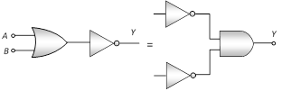
question_answer26) Assertion : The following circuit represents 'OR' gate Reason : For the above circuit \[Y=\bar{X}=\overline{\overline{A+B}}=A+B\]
question_answer27) Assertion : A P-N photodiode is made from a semiconductor for which Eg = 2.8 eV. This photo diode will not detect the wavelength of 6000 nm. Reason : A PN photodiode detect wavelength l if \[\frac{hc}{\lambda }>{{E}_{g}}\].
question_answer28) Assertion : 29 is the equivalent decimal number of binary number 11101. Reason : (11101)2 = (1 ´ 24 + 1 ´ 23 + 1 ´ 22 + 0 ´ 21 + 1 ´ 20 )10 = (16 + 8 + 4 + 0 + 1)10 = (29)10
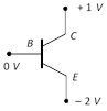
question_answer29) Assertion : When PN-junction is forward biased then motion of charge carriers at junction is due to diffusion. In reverse biasing. The cause of motion of charge is drifting. Reason : In the following circuit emitter is reverse biased and collector is forward biased.
question_answer30) Assertion : De-morgan's theorem \[\overline{A+B}=\bar{A}\cdot \bar{B}\] may be explained by the following circuit Reason : In the following circuit, for output inputs ABC are 101
question_answer31) Assertion : In the following circuit the potential drop across the resistance is zero. Reason : The given resistance has low value.
Please Wait you are being redirected....
You need to login to perform this action.You will be redirected in 3 sec
OTP has been sent to your mobile number and is valid for one hour
Your mobile number is verified.


 Reason : In the following circuit, for output inputs ABC are 101
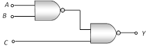
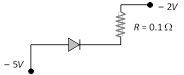 Reason : The given resistance has low value.