Field-Effect Transistor
Category : JEE Main & Advanced
The low input impedance of the junction transistor is a handicap in certain applications. In addition, it is difficult to incorporate large numbers of them in an integrated circuit and they consume relatively large amounts of power. The field-effect transistor (FET) lacks these disadvantages and is widely used today although slower in operation than junction transistors.
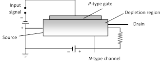
An n-channel FET consists of a block of N-type material with contacts at each end together with a strip of P-type material on one side that is called the gate. When connected as shown, electrons move from the source terminal to the drain terminal through the N-type channel. the PN junction is given a reverse bias, and as a result both the N and P materials near the junction are depleted on charge carriers. The higher the reverse potential on the gate, the larger the depleted region in the channel and the fewer the electrons available to carry the current. Thus the gate voltage controls the channel current. Very little current passes through the gate circuit owing to the reverse bias, and the result is an extremely high input impedance. FET is uni-polar.


You need to login to perform this action.
You will be redirected in
3 sec

