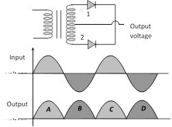
 The contribution to output voltage from diode ? 2 is [MP PMT 2001]
A) A, C
B) B, D
C) B, C
D) A, D
Correct Answer: B
Solution :
In the positive half cycle of input ac signal diode D1 is forward biased and D2 is reverse biased so in the output voltage signal, A and C are due to D1. In negative half cycle of Input ac signal D2 conducts, hence output signals B and D are due to D2.


You need to login to perform this action.
You will be redirected in
3 sec

