| (i) Distinguish between metals, insulators and semiconductors on the basis of energy bank diagram. |
| (ii) Draw a circuit diagram showing the biasing of an LED. State the factor which controls |
| (a) wavelength of light, |
| (b) intensity of light emitted by the diode. |
| Or |
| (i) What is the difference between an intrinsic semiconductor and p-type semiconductor. Explain, why a p-type semiconductor is electrically neutral, although \[{{n}_{h}}>>{{n}_{e}}?\] |
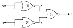
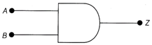
| (ii) In the figure given below, analyse the action of the gates (1) and (2) and identify the logic gate of the complete circuit so obtained. Give its symbol and the truth table. |
 |
Answer:
(i) Three types of energy band diagrams have been shown in figure. From these we conclude as follows Metals In metals, conduction and valence bands are overlapping. It is the case of a metal where energy band gap \[{{E}_{g}}=0.\] In such a case, a large number of electrons are available for electrical conduction and hence, the resistivity of such materials is low or the conductivity is high. 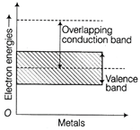 Insulators In insulators, there is a large band gap \[({{E}_{g}}>3\,eV)\] between valence and conduction bands and there are no electrons in conduction band. On account of large band gap electrons cannot be excited from valence band to the conduction band and hence the substance behaves as an insulator.
 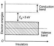 Semiconductors In semiconductors, energy band gap \[{{E}_{g}}\] is small \[({{E}_{g}}<3\,eV)\] and of the order 1 eV. Because of the small band gap, at any temperature, other than 0 K, some electrons can be thermally excited to the conduction band and these excited electrons can move in the conduction band. Hence, the resistance is not as high as that of the insulators. This is the case of semiconductors.
 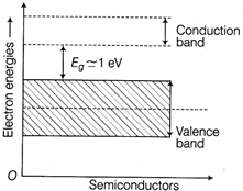 Circuit Diagram of LED
 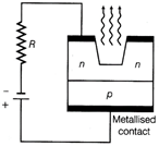 A forward biased LED (ii) (a) Wavelength of light controlled by band gap \[({{E}_{g}})\] of semiconductor material. (b) Intensity of emitted light by the diode depends on concentration of impurity in junction diode. Or (i) The difference between intrinsic and p-type extrinsic semiconductors are as
A p-type semiconductor crystal is electrically neutral because the charge of additional charge carriers (i.e. holes) is just equal and opposite to that of the ionised cores in the crystal lattice. (ii) Gates (1) and (2) are both NOR gates, whose both the inputs have been joined together. As, a result gates (1) and (2) behave as NOT gates and invert the input signals A and B i.e. give outputs of \[\overline{A}\] and \[\overline{B},\] respectively It means that \[\overline{A}=X\] and \[\overline{B}=Y.\] Gate (3) is also a NOR gate. Hence, the truth table of given circuit is given below.
Intrinsic semiconductors
p-type extrinsic semiconductors
These are pure semiconducting material and no impurity of any sort is added to them. \[Consequently{{n}_{e}}={{n}_{h}}={{n}_{i}}.\]
These are prepared by doping a small quantity of impurity of trivalent material to the pure semiconducting material. As a result, \[{{n}_{h}}>>{{n}_{e}}.\]
The electrical conductivity is generally small and a function of temperature alone.
The electrical conductivity is comparatively high and mainly a function of amount of doping.
The circuit carries out the logic operation of an AND gate. Logic symbol of an AND gate is as shown below.
A
B
X
Y
Z
0
0
1
1
0
0
1
1
0
0
1
0
0
1
0
1
1
0
0
1


You need to login to perform this action.
You will be redirected in
3 sec

