| Explain the formation of depletion layer and potential barrier in a p-n junction with the help of diagram and also with the help of a labelled diagram, explain the use of p-n junction diode as full wave rectifier. Draw the input and output waveforms. |
| OR |
| (i) Explain briefly, with the help of a circuit diagram, how V-I characteristics of a p-n junction diodes are obtained in |
| (a) forward bias |
| (b) reverse bias? |
| Draw the shape of the curves obtained. |
| (ii) A photodiode is fabricated from a semiconductor with a band gap of 2.8 eV Can it detect wavelength of 6000 nm? Justify. |
Answer:
The small region in the vicinity of the junction which is free from free charge carriers and has only immobile ions is called the depletion layer. 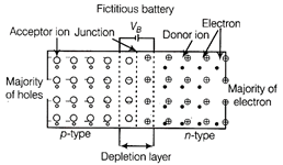 p-n junction diagram When p-n junction is formed, majority charge carriers begin to diffuse from higher concentrations to lower concentrations. Thus, electron diffuses from n-type to p-type whereas hole diffuses from p-type to n-type semiconductor. This leads to electron-hole pair annihilation. As a result, near the junction, p-region is left with negative ions whereas n-region is left with positive ions. This produces potential difference across the junction which opposes the further diffusion of charge carriers. This potential difference is known as potential barrier. A full wave rectifier takes input in the primary coil of a centre tapped transformer. Two junction-diodes \[{{D}_{1}}\] and \[{{D}_{2}}\] and a load resistance \[{{R}_{L}}\] are connected with the centre tapped secondary coil of transformer as shown in the figure. Let during the first positive half cycle of input AC given in figure below, the end A is positive and end B is negative relative to the centre T. This makes diode \[{{D}_{1}}\] in forward bias and \[{{D}_{2}}\] in reverse bias and current in \[{{R}_{L}}\] flows from X to Y. Similarly for next negative half cycle of input AC, \[{{D}_{2}}\] conducts being in forward bias but \[{{D}_{1}}\] does not. Again the current in \[{{R}_{L}}\] flows from X to Y. Thus, unidirectional pulsative direct current is obtained through \[{{R}_{L}}\] during both the half cycles of input AC. This process is termed as full wave rectification and diodes are referred as full wave rectifiers. Junction diode full wave rectifier
 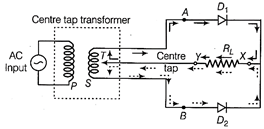 Input and output waveforms
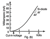
 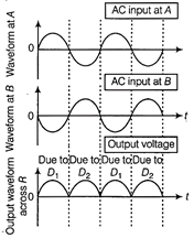 Or (i) (a) Forward bias characteristics Fig. (a) shows circuit diagram for junction diode characteristics in forward bias. It is observed that initially no current flows upto cut-in-voltage. After cut-in-voltage, current increases rapidly as depicted in Fig. (b).
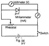
 Voltage and current variation graph (b) Reverse bias characteristics Fig. (c) represents junction diode in reverse bias and Fig. (d) represents characteristic curve in reverse bias.
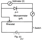
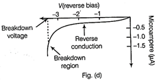 Variation of current through p-n junction In reverse bias, a microammeter is used to measure current as reverse current is very feeble. A graph showing the variation of current flowing through a p-n junction with the voltage applied across it, is known as characteristic curve. (ii) Wavelength, \[\lambda =6000nm\] Energy of incident photon \[E=hv=\frac{hc}{\lambda }\] \[=\frac{6.6\times {{10}^{-34}}\times 3\times {{10}^{8}}}{600\times {{10}^{-9}}}J\] \[=\frac{3.3\times {{10}^{-20}}}{1.6\times {{10}^{-19}}}eV\] \[\Rightarrow \] \[E=0.207eV\] Energy required to cross the gap \[{{E}_{g}}=2.8eV\] \[\therefore E<{{E}_{g,}}\] the p-n junction cannot detect the given wavelength of 6000 nm.


You need to login to perform this action.
You will be redirected in
3 sec

