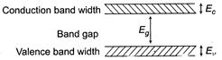
question_answer9) The electrical conductivity of a semiconductor increases when electromagnetic radiation of wavelength shorter than 2480 nm, is incident on it. The band gap for the semiconductor is [AIEEE 2005]
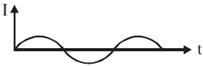
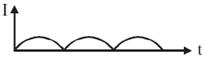
question_answer11) In a full wave rectifier, circuit operating from 50 Hz mains frequency, the fundamental frequency in the ripple would be [AIEEE 2005]
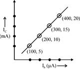
question_answer12) In a common-base mode of a transistor, the collector current is 5.488 mA for an emitter current of 5.60 mA. The value of the base current amplification factor (P) will be [AIEEE 2006]
question_answer17) Carbon, silicon and germanium have four valence electrons each. At room temperature, which one of the following statements is most appropriate? [AIEEE 2007]
A)
The number of free conduction electrons is significant in C but small in Si and
doneclear
B)
The number of free conduction electrons is negligibly small in all the three
doneclear
C)
The number of free electrons for conduction is significant in all the three
doneclear
D)
The number of free electrons for conduction is significant only inandbut small in C
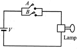
question_answer18) A working transistor with its three legs marked P, Q and R is tested using a multimeter. No conduction is found between P and Q. By connecting the common (negative) terminal of the multimeter to R and the other (positive) terminal to P or Q, some resistance is seen on the multimeter. Which of the following is true for the transistor? [AIEEE 2008]
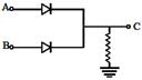
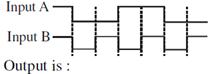
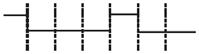
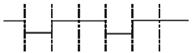
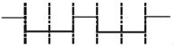
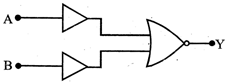
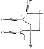
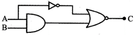
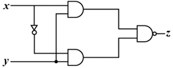
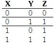
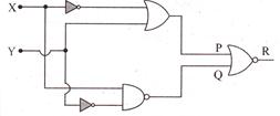
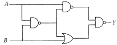
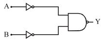
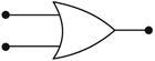
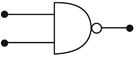
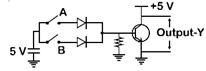
Consider two transistors as shown in figure. If 0 `volts corresponds to false and 5Volts correspond to true then the output at corresponds to: [JEE ONLINE 09-04-2013
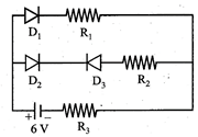
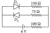
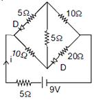
Figure shows a circuit in which three identical diodes are used. Each diode has forward resistance of 20 and infinite backward resistance. Resistors . Battery voltage is 6 V. The current though . [JEE ONLINE 22-04-2013]
question_answer36) An n-p-n transistor has three leads A, B and C. Connecting B and C by moist fingers, A to the positive lead of an ammeter, and C to the negative lead of the ammeter, one finds large deflection. Then, A, B and C refer respectively to: [JEE ONLINE 09-04-2014]
question_answer38) For LEDs to emit light in visible region of electromagnetic light, it should have energy band gap in the range of: [JEE ONLINE 12-04-2014]
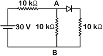
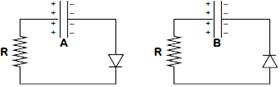
A 2V battery is connected across AB as shown in the figure. The value of the current supplied by the battery when in one case battery's positive terminal is connected to A and in other case when positive terminal of battery is connected to B will respectively be : [JEE MAIN 11-04-2015]
question_answer43) For a common emitter configuration, if and have their usual meanings, the incorrect relationship betweenandis [JEE MAIN - I 3-4-2016]
question_answer46) An unknown transistor needs to be identified as npn or pnp type. A multi meter, with +ve and -ve terminals, is used to measure resistance between different terminals transistor. If terminal 2 is the base of the transistor then which of the following is correct for a pnp transistor? [JEE ONLINE 09-04-2016]
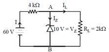
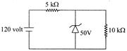
question_answer47) An experiment is performed to determine the I - V characteristics of a Zener diode, which has a protective resistance of and maximum power of dissipation rating of 1W. The minimum voltage range of the DC source in the circuit is: [JEE ONLINE 09-04-2016]
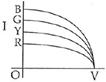
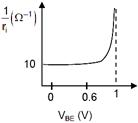
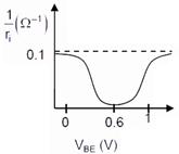
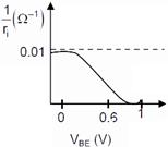
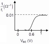
question_answer49) A realistic graph depicting the variation of the reciprocal of input resistance in an input characteristics measurement in a common emitter transistor configuration is: [JEE ONLINE 10-04-2016]
question_answer51) The ratio (R) of output resistance , and the input resistance in measurements of input and output characteristics of a transistor is typically in the range: [JEE ONLINE 10-04-2016]
question_answer52) In a common emitter amplifier circuit using an n-p-n transistor, the phase difference between the input and the output voltages will be: [JEE Main 2017]
question_answer53) What is the conductivity of a semiconductor sample having electron concentration of hole concentration of electron mobility of and hole mobility of (Take charge of electron as ) [JEE Online 08-04-2017]
question_answer55) The current gain of a common emitter amplifier is 69. If the emitter current is 7.0 mA, collector current is- [JEE Online 09-04-2017]
In a common emitter configuration with suitable bias, it is given than \[{{R}_{L}}\] is the load resistance and \[{{R}_{BE}}\] is small signal dynamic resistance (input side). Then, voltage gain, current gain and power gain are given, respectively, by: [JEE Online 15-04-2018]
\[\beta \] is current gain, \[{{I}_{B}},{{I}_{C}},{{I}_{E}}\] are respectively base, collector and emitter currents:
question_answer60) Mobility of electrons in a semiconductor is defined as the ratio of their drift velocity to the applied electric field. If, for an n-type semiconductor, the density of electrons is and their mobility is then the resistivity of the semiconductor (since it is an n-type semiconductor contribution of holes is ignored) is close to: [JEE Main 09-Jan-2019 Morning]
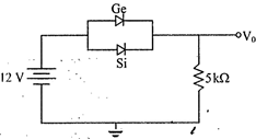
Ge and Si diodes start conducting at 0.3 V and 0.7 V respectively. In the following figure if Ge diode connection are reversed, the value of changes by: (assume that the Ge diode has large breakdown voltage)
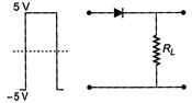
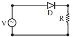
The circuit shown below contains two ideal diodes, each with a forward resistance of If the battery voltage is 6 V, the current through the resistance (in Amperes) is [JEE Main 11-Jan-2019 Evening]
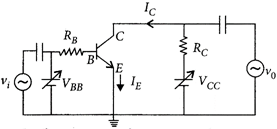
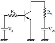
In the figure, given that supply can vary from 0 to and The minimum base current and the input voltage at which the transistor will go to saturation, will be respectively [JEE Main 12-Jan-2019 Evening]
question_answer69) An NPN transistor is used in common emitter configuration as an amplifier with load resistance. Signal voltage of 10 mV is applied across the base-emitter. This produces a 3 mA change in the collector current and change in the base current of the amplifier. The input resistance and voltage gain are: [JEE Main 9-4-2019 Morning]
question_answer71) An npn transistor operates as a common emitter amplifier, with a power gain of 60 dB. The input circuit resistance is and the output load resistance is The common emitter current gain b is : [JEE Main 10-4-2019 Morning]
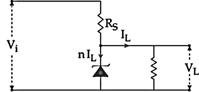
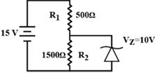
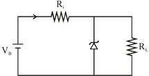
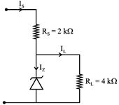
The figure represents a voltage regulator circuit using a Zener diode. The breakdown voltage of the Zener diode is 6V and the load resistance is The series resistance of the circuit is If the battery voltage varies from 8V to 16V, what are the minimum and maximum values of the current through Zener diode? [JEE Main 10-4-2019 Afternoon]
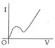
The transfer characteristic curve of a transistor, having input and output resistance and respectively, is shown in the figure. The Voltage and Power gain, are respectively : [JEE Main Held on 12-4-2019 Morning]
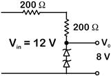
Figure shown a DC voltage regulator circuit, with a Zener diode of breakdown voltage = 6V. If the unregulated input voltage varies between 10 V to 16 V, then what is the maximum Zener current? [JEE Main 12-4-2019 Afternoon]
Both the diodes used in the circuit shown are assumed to be ideal and have negligible resistance when these are forward biased. Built in potential in each diode is 0.7 V. For the input voltages shown in the figure, the voltage (in Volts) at point A is ___________ [JEE MAIN Held on 09-01-2020 Morning]
Two identical capacitors A and B, charged to the same potential 5V are connected in two different circuits as shown below at time t = 0. If the charge on capacitors A and B at time t = CR is \[{{Q}_{A}}\] and \[{{Q}_{B}}\] respectively, then (Here e is the base of natural logarithm) [JEE MAIN Held on 09-01-2020 Evening]
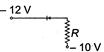
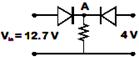
The circuit shown below is working as a \[8\text{ }V\text{ }dc\]regulated voltage source. When 12 V is used as input, the power dissipated (in mW) in each diode is; (considering both zener diodes are identical) ______.


 [JEE MAIN 11-04-2015]
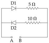

 *-correct-answer-description-* [b] Factual


 [JEE MAIN Held on 09-01-2020 Evening]