Solved papers for NEET Physics Semiconducting Devices NEET PYQ-Semiconducting Devices

done NEET PYQ-Semiconducting Devices Total Questions - 96

  • question_answer1) The cause of the potential barrier in a \[p-n\] diode is:                                             [AIPMT 1998]

    A)
     depletion of positive charges near the junction

    B)
    concentration of positive charges near the junction

    C)
    depletion of negative charges near the junction

    D)
     concentration of positive and negative charges near the junction

    View Answer play_arrow
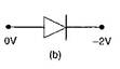
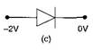
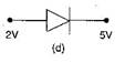
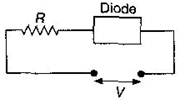
  • question_answer2) A semi-conducting device is connected in a series in circuit with a battery and a resistance. A current is allowed to pass through the circuit. If the polarity of the battery is reversed, the current drops to almost zero. The device may be:                                                                                                                                                            [AIPMT 1998]

    A)
           a \[p-n\] junction

    B)
          an intrinsic semiconductor

    C)
     a \[p-\]type semiconductor

    D)
          an \[n-\]type semiconductor

    View Answer play_arrow
  • question_answer3)             The transfer ratio \[\beta \] of a transistor is 50. The input resistance of the transistor when used in the common emitter configuration is \[1\,k\,\Omega \]. The peak value of the collector AC current for an AC input voltage of 0.01 V peak is:                                                                                                                                              [AIPMT 1998]

    A)
     \[100\,\mu A\]  

    B)
          \[0.01\,mA\]     

    C)
     \[0.25\,mA\]     

    D)
          \[500\,\mu A\]

    View Answer play_arrow
  • question_answer4) 
    Which one of the following gates will have an output of 1?                                                    [AIPMT 1998]


    A)
           A                    

    B)
          B

    C)
     C        

    D)
                      D

    View Answer play_arrow
  • question_answer5) The truth table given below is for which gate?                                          [AIPMT 1998]
    Input Output
    A B C
    0 0 1
    0 1 1
    1 0 1
    1 1 0

    A)
     XOR   

    B)
                      OR

    C)
     AND

    D)
                      NAND

    View Answer play_arrow
  • question_answer6) Which of the following when added as an impurity into silicon produces n-type semiconductor?             [AIPMT 1999]

    A)
     P        

    B)
                      Al

    C)
     B        

    D)
                      Mg

    View Answer play_arrow
  • question_answer7) In a junction diode, the holes are due to:                                                                [AIPMT 1999]

    A)
     protons 

    B)
    extra electrons

    C)
     neutrons 

    D)
     missing electrons

    View Answer play_arrow
  • question_answer8) Depletion layer consists of:                                                                                       [AIPMT 1999]

    A)
     electrons

    B)
                      protons

    C)
          mobile charge carriers                

    D)
     immobile ions

    View Answer play_arrow
  • question_answer9) In forward bias the width of depletion layer in a p-n junction diode:                                          [AIPMT 1999]

    A)
     increases          

    B)
          decreases

    C)
     remains constant

    D)
          first increases then decreases

    View Answer play_arrow
  • question_answer10) In p-type semiconductor, the major charge carriers are:                                                               [AIPMT 1999]

    A)
     holes                

    B)
          electrons

    C)
     protons 

    D)
    neutrons

    View Answer play_arrow
  • question_answer11) Sodium has body centred packing. If the distance between two nearest atoms is \[3.7\overset{o}{\mathop{A}}\,\] then the lattice parameter is:                                                                                                          [AIPMT 1999]

    A)
     \[3.3\,\overset{o}{\mathop{A}}\,\]

    B)
                      \[3.9\,\overset{o}{\mathop{A}}\,\]

    C)
     \[4.3\,\overset{o}{\mathop{A}}\,\]

    D)
                      \[4.8\,\overset{o}{\mathop{A}}\,\]

    View Answer play_arrow
  • question_answer12) 
    The following circuit represents:                                                                                               [AIPMT 1999]

    A)
                 OR gate

    B)
                   XOR gate

    C)
          AND gate

    D)
      NAND gate

    View Answer play_arrow
  • question_answer13) If \[\alpha \] and \[\beta \] are current gains in common-base and common-emitter configurations of a transistor, then \[\beta \] is equal to:

    A)
     \[\frac{1}{\alpha }\]     

    B)
                      \[\frac{\alpha }{1+\alpha }\]

    C)
     \[\frac{\alpha }{1-\alpha }\]

    D)
                      \[\alpha -\frac{1}{\alpha }\]

    View Answer play_arrow
  • question_answer14) The truth table given below:                                                                                                       [AIPMT 2000]
    Inputs Output
    A B Y
    0 0 0
    1 0 0
    0 1 0
    1 1 1
                represents:

    A)
     AND gate

    B)
        NOR gate

    C)
          OR gate 

    D)
    NAND gate

    View Answer play_arrow
  • question_answer15) In which of the following figures, junction diode is forward biased                              [AIPMT 2000]

    A)

    B)
                  

    C)

    D)
        

    View Answer play_arrow
  • question_answer16) In a common-base configuration of a transistor \[\frac{\Delta {{i}_{C}}}{\Delta {{i}_{E}}}=0.98\] then current gain in common emitter configuration of transistor will be:                                                              [AIPMT 2001]

    A)
     49       

    B)
                      98                   

    C)
     4.9      

    D)
                      24.5

    View Answer play_arrow
  • question_answer17) 
    If internal resistance of cell is negligible, then current flowing through the circuit is:        [AIPMT 2001]

    A)
    \[\frac{3}{50}\,A\]

    B)
                      \[\frac{5}{50}\,A\]

    C)
     \[\frac{4}{50}A\]

    D)
                      \[\frac{2}{50}\,A\]

    View Answer play_arrow
  • question_answer18) 
    The truth table given below represents:                                                                         [AIPMT 2001]
    Input Output
    A B Y
    1 1 0
    0 1 1
    1 0 1
    0 0 1
               

    A)
    NOT gate

    B)
         OR gate

    C)
          XOR gate

    D)
                     NAND gate

    View Answer play_arrow
  • question_answer19) In bcc structure of lattice constant \['a',\] the minimum distance between atoms is:                               [AIPMT 2001]

    A)
     \[\frac{\sqrt{3}}{2}\,a\]

    B)
                      \[\sqrt{2}a\]

    C)
     \[\frac{a}{\sqrt{2}}\]    

    D)
                      \[\frac{a}{2}\]

    View Answer play_arrow
  • question_answer20) The number of atoms per unit cell in bcc lattice is:                                                                    [AIPMT 2002]

    A)
     1        

    B)
         2         

    C)
          4      

    D)
                      9

    View Answer play_arrow
  • question_answer21) For a transistor \[\frac{{{I}_{C}}}{{{I}_{E}}}=0.96,\] the current gain in common-emitter configuration is [AIPMT 2002]

    A)
     6       

    B)
      12      

    C)
     24    

    D)
     48

    View Answer play_arrow
  • question_answer22) For conduction in a \[p-n\] junction, the biasing is:                                                               [AIPMT 2002]

    A)
     high potential on n-side and low potential on p-side

    B)
          high potential on p-side and low potential on n-side                                   

    C)
          same potential on both p and n-sides

    D)
     undetermined

    View Answer play_arrow
  • question_answer23) 
    For a given circuit of ideal \[p-n\] junction diode, which of the following is correct?  [AIPMT 2002]

    A)
           In forward biasing the voltage across R is V

    B)
     In reverse biasing the voltage across R Is 2V

    C)
          In forward biasing the voltage across R is 2V

    D)
          In reverse biasing the voltage across R is 2V

    View Answer play_arrow
  • question_answer24) 
    The truth table for a logic gate is:
    Input Output
    A B Y
    1 1 0
    0 1 1
    1 0 1
    0 0 1
    The logic gate is:                                                                                                     [AIPMT 2002]

    A)
           NAND gate    

    B)
      XOR gate

    C)
     NOR gate     

    D)
    OR gate

    View Answer play_arrow
  • question_answer25)             Reverse bias applied to a junction diode:                                                                            [AIPMT 2003]

    A)
     increases the majority carrier current

    B)
          increases the minority carrier current

    C)
          lowers the potential barrier          

    D)
          raises the potential barrier

    View Answer play_arrow
  • question_answer26) 
    Following diagram performs the logic function of:                                      [AIPMT 2003]

    A)
           OR gate           

    B)
          AND gate

    C)
     XOR gate

    D)
         NAND gate

    View Answer play_arrow
  • question_answer27) Barrier potential of a \[p-n\] junction diode does not depend on:                               [AIPMT 2003]

    A)
     forward bias

    B)
     doping density

    C)
          diode design

    D)
      temperature

    View Answer play_arrow
  • question_answer28) If a full wave rectifier circuit is operating from 50 Hz mains, the fundamental frequency in the ripple will be: [AIPMT 2003]

    A)
     70.7 Hz 

    B)
          100 Hz

    C)
          25 Hz 

    D)
          59 Hz

    View Answer play_arrow
  • question_answer29) A \[n-p-n\] transistor conducts when:                                                                      [AIPMT 2003]

    A)
     collector is positive and emitter is at same potential as the base

    B)
          both collector and emitter are negative with respect to the base

    C)
          both collector and emitter are positive with respect to the base

    D)
          collector is positive and emitter is negative with respect to the base

    View Answer play_arrow
  • question_answer30) In semiconductors at a room temperature:                                                                          [AIPMT (S) 2004]

    A)
           the valence band is partially empty and the conduction band is partially filled

    B)
          the valence band is completely filled and the conduction band is partially filled

    C)
          the valence band is completely filled

    D)
          the conduction band is completely empty

    View Answer play_arrow
  • question_answer31) The output of OR gate is 1:                                                                       [AIPMT (S) 2004]

    A)
     only if both inputs are zero

    B)
          if either or both inputs are 1

    C)
          only if both inputs are 1

    D)
          if either input is zero

    View Answer play_arrow
  • question_answer32) In a \[p-n\] junction photo cell, the value of the photo-electromotive force produced by monochromatic light is proportional to:                                                                                                                        [AIPMT (S) 2004]

    A)
           the barrier voltage at the \[p-n\] junction

    B)
     the intensity of the light falling on the cell

    C)
          the frequency of the light falling on the cell

    D)
          the voltage applied at the \[p-n\] junction

    View Answer play_arrow
  • question_answer33) Of the diodes shown in the following diagrams, which one is reverse biased?                 [AIPMT (S) 2004]

    A)
                  

    B)

    C)
     

    D)
     

    View Answer play_arrow
  • question_answer34)   Application of a forward bias to a \[p-n\]  junction:                                                  [AIPMT (S) 2005]

    A)
           increases the number of donors on the n-side

    B)
          increases the electric field in the depletion zone

    C)
          increases the potential difference across the depletion zone

    D)
          widens the depletion zone

    View Answer play_arrow
  • question_answer35) Zener diode is used for:                                                                                                       [AIPMT (S) 2005]

    A)
     producing oscillations in an oscillator       

    B)
     amplification

    C)
     stabilization      

    D)
     rectification

    View Answer play_arrow
  • question_answer36) Carbon, silicon and germanium atoms have four valence electrons each. Their valence and conduction bands are separated by energy band gaps represented by \[{{({{E}_{g}})}_{C}},\] \[{{({{E}_{g}})}_{Si}}\] and \[({{E}_{g}}){{G}_{Ge}}\] respectively. Which one of the following relationships is true in their case?                                           [AIPMT (S) 2005]

    A)
    \[{{({{E}_{g}})}_{C}}>{{({{E}_{g}})}_{Si}}\]

    B)
          \[{{({{E}_{g}})}_{C}}={{({{E}_{g}})}_{Si}}\]

    C)
     \[{{({{E}_{g}})}_{C}}<({{E}_{g}})Ge\]         

    D)
     \[{{({{E}_{g}})}_{C}}<{{({{E}_{g}})}_{Si}}\]

    View Answer play_arrow
  • question_answer37) Choose the only false statement from the following:                                       [AIPMT (S) 2005]

    A)
     Substances with energy gap of the order of 10 eV are insulators

    B)
          The conductivity of a semiconductor increases with increases in temperature

    C)
          In conductors the valence and conduction bands may overlap

    D)
          The resistivity of a semiconductor increases with increase in temperature

    View Answer play_arrow
  • question_answer38) Copper has face-centered cubic (fcc) lattice with interatomic spacing equal to \[2.54\,\overset{o}{\mathop{A}}\,\]. The value of lattice constant for this lattice is:                                                                           [AIPMT (S) 2005]

    A)
           \[1.27\,\overset{o}{\mathop{A}}\,\]       

    B)
          \[5.08\,\overset{o}{\mathop{A}}\,\]

    C)
     \[2.54\,\overset{o}{\mathop{A}}\,\]

    D)
                      \[3.59\,\overset{o}{\mathop{A}}\,\]

    View Answer play_arrow
  • question_answer39) A transistor-oscillator using a resonant circuit with an inductor L (of negligible resistance) and a capacitor C in series produce oscillations of frequency f. If L is doubled and C is changed to 4C, the frequency will be:     [AIPMT (S) 2006]

    A)
     \[f/4\]              

    B)
     \[8f\]

    C)
     \[f/2\sqrt{2}\]   

    D)
          \[f/2\]

    View Answer play_arrow
  • question_answer40) A transistor is operated in common emitter configuration at constant collector voltage \[{{V}_{c}}=1.5\text{ }V\] such that a change in the base current from \[100\,\,\mu A\]  to \[150\,\,\mu A\] produces a change in the collector current from 5 mA to 10 mA. The current gain \[(\beta )\] is:                                                                                     [AIPMT (S) 2006]

    A)
     67     

    B)
                      75       

    C)
     100  

    D)
     50

    View Answer play_arrow
  • question_answer41) A forward biased diode is:

    A)
      The Boolean expression which satisfies the output of this logic gate is \[C=A\]. B, which is for AND gate

    B)
     

    C)
     

    D)
                 

    View Answer play_arrow
  • question_answer42) 
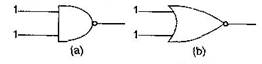
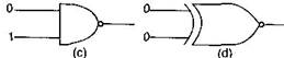
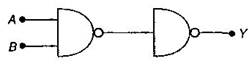
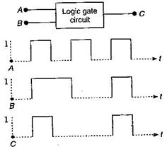
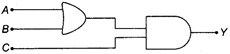
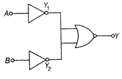
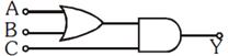
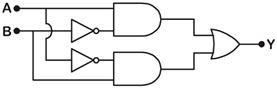
    The following figure shows a logic gate circuit with two inputs A and B and the output C. The voltage waveforms of A, B and C are as shown below:                                                                                      [AIPMT (S) 2006]
               
    The logic circuit gate is:

    A)
     AND gate                     

    B)
     NAND gate      

    C)
     NOR gate

    D)
                      OR gate

    View Answer play_arrow
  • question_answer43) 
    In the following circuit, the output Y for all possible inputs A and B is expressed by the truth table: [AIPMT (S) 2007]                                        

    A)
                            A          B          Y
                            0          0          0
                            0          1          0
                            1          0          0
                            1          1          1

    B)
                            A          B          Y                         0          0          1                         0          0          1                         1          0          1                         1          1          0

    C)
                            A          B         Y                         0          0          1                         0          1          0                                              1          0          0                         1          1          0

    D)
                            A          B          Y                         0          0          0                         0          1          1                         1          1          1

    View Answer play_arrow
  • question_answer44) 
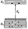
    In the energy band diagram of a material shown below, the open circles and filled circles denote holes and electrons respectively. The material is a/an:                                                                                             [AIPMT (S) 2007]

    A)
           p-type semiconductor    

    B)
     insulator

    C)
          metal

    D)
     n-type semiconductor

    View Answer play_arrow
  • question_answer45) For a cubic crystal structure which one of the following relations indicating the cell characteristic is correct?[AIPMT (S) 2007]

    A)
     \[a\ne b\ne c\] and \[\alpha \ne \beta \] and \[\gamma \ne {{90}^{o}}\]    

    B)
          \[a\ne b\ne c\] and \[\alpha =\beta =\gamma ={{90}^{o}}\]

    C)
          \[a=b=c\] and \[\alpha \ne \beta \ne \gamma ={{90}^{o}}\]

    D)
          \[a=b=c\] and \[\alpha =\beta =\gamma ={{90}^{o}}\]

    View Answer play_arrow
  • question_answer46) A common emitter amplifier has a voltage gain of 50, an input impedance of \[100\,\Omega \] and an output impedance of \[200\,\Omega \]. The power gain of the amplifier is:                                                        [AIPMT (S) 2007]

    A)
     500                 

    B)
          1000   

    C)
     1250 

    D)
     100

    View Answer play_arrow
  • question_answer47) If the lattice parameter for a crystalline structure is \[3.6\,\,\overset{o}{\mathop{A}}\,,\] then the atomic radius in fee crystal is                                                                                                            [AIPMPT (S) 2008]

    A)
     \[1.81\,\overset{o}{\mathop{A}}\,\]

    B)
                      \[2.10\,\overset{o}{\mathop{A}}\,\]

    C)
     \[2.92\,\overset{o}{\mathop{A}}\,\]       

    D)
          \[1.27\,\overset{o}{\mathop{A}}\,\]

    View Answer play_arrow
  • question_answer48) The voltage gain of an amplifier with 9% negative feedback is 10. The voltage gain without feedback will be                                                                                                                                              [AIPMPT (S) 2008]

    A)
     90         

    B)
      10

    C)
                      1.25    

    D)
     100

    View Answer play_arrow
  • question_answer49) A \[p-n\] photodiode is made of a material with a band gap of 2.0 eV. The minimum frequency of the radiation that can be absorbed by the material is nearly                                                                                           [AIPMPT (S) 2008]

    A)
     \[10\times {{10}^{14}}Hz\]                 

    B)
     \[5\times {{10}^{14}}Hz\]

    C)
     \[1\times {{10}^{14}}Hz\]       

    D)
          \[20\times {{10}^{14}}Hz\]

    View Answer play_arrow
  • question_answer50) 
    The circuit is equivalent to                                                                         [AIPMPT (S) 2008]

    A)
     AND gate   

    B)
     NAND gate

    C)
     NOR gate   

    D)
     OR gate

    View Answer play_arrow
  • question_answer51) A \[p-n\] photodiode is fabricated from .a semiconductor with a band gap of 2.5 eV. It can detect a signal of wavelength                                                                                                                          [AIPMT (S) 2009]

    A)
     \[6000\,\overset{o}{\mathop{A}}\,\]      

    B)
     4000 nm          

    C)
     6000 nm                      

    D)
     \[4000\,\overset{o}{\mathop{A}}\,\]

    View Answer play_arrow
  • question_answer52) 
    The symbolic representation of four logic gates                                        [AIPMT (S) 2009]
    (i)                                 (ii)
           
    (iii)                                (iv)
            
    The logic symbols for OR, NOT and NAND gates are respectively

    A)
     (iii), (iv), (ii)   

    B)
     (iv), (i), (iii)

    C)
     (iv), (ii), (i) 

    D)
     (i), (iii), (iv)

    View Answer play_arrow
  • question_answer53) A transistor is operated in common-emitter configuration at \[{{V}_{c}}=2\] volt such that a change in the base current from \[100\,\mu A\] to \[200\,\mu A\]produces a change in the collector current from 5 mA to 10 mA. The current gain is                                                                                                                                            [AIPMT (S) 2009]

    A)
     75

    B)
                 100                

    C)
     150        

    D)
     50

    View Answer play_arrow
  • question_answer54) Sodium has body centred packing. Distance between two nearest atoms is 3.7 A. The lattice parameter is [AIPMT (S) 2009]

    A)
     \[6.8\,\,\overset{o}{\mathop{A}}\,\]                   

    B)
     \[4.3\,\,\overset{o}{\mathop{A}}\,\]

    C)
     \[3.0\,\,\overset{o}{\mathop{A}}\,\]       

    D)
          \[8.6\,\,\overset{o}{\mathop{A}}\,\]

    View Answer play_arrow
  • question_answer55) Which one of the following statement is false?                                                         [AIPMT (S) 2010]

    A)
     Pure Si doped with trivalent impurities gives a p-type semiconductor

    B)
     Majority carriers in a n-type semiconductor are holes

    C)
     Minority carriers in a p-type semiconductor are electrons

    D)
     The resistance of intrinsic semiconductor decreases with increase of temperature

    View Answer play_arrow
  • question_answer56) The device that can act as a complete electronic circuit is                                 [AIPMT (S) 2010]

    A)
     Junction diode

    B)
          Integrated circuit

    C)
     Junction transistor

    D)
         Zener diode

    View Answer play_arrow
  • question_answer57) 
    To get an output \[Y=1\] from the circuit shown below, the input must be      [AIPMT (S) 2010]

    A)
    A          B          C  0         1          0

    B)
     0         0          1

    C)
      1        0          1

    D)
     1         0          0

    View Answer play_arrow
  • question_answer58) 
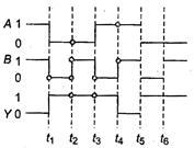
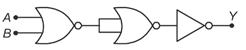
    The following figure shows a logic gate circuit with two inputs A and B and the output Y. The voltage waveforms of A, B and Y are as given                                                                                                                [AIPMT (M) 2010]
     The logic gate is

    A)
     NOR gate        

    B)
          OR gate           

    C)
     AND gate    

    D)
     NAND gate

    View Answer play_arrow
  • question_answer59) 
    For transistor action
    (1) Base, emitter and collector regions should have   similar   size    and   doping concentrations.
    (2) The base region must be very thin and lightly doped.
    (3) The emitter-base junction is forward biased and base-collector junction is reverse biased.
    (4) Both the emitter-base junction as well as the base collector junction are forward biased.
    Which one of the following pairs of statements is correct?

    A)
     (4) and (1)       

    B)
     (1) and (2)       

    C)
     (2) and (3)  

    D)
      (3) and (4)

    View Answer play_arrow
  • question_answer60) 
    In the following figure, the diodes which are forward biased, are            [AIPMT (M) 2011]


    A)
     C only      

    B)
     C and A

    C)
          B and D      

    D)
     A, B and D

    View Answer play_arrow
  • question_answer61) Pure Si at 500 K has equal number of electron \[({{n}_{e}})\]and hole \[({{n}_{h}})\] concentrations of \[1.5\times {{10}^{16}}{{m}^{-3}}\]. Doping by indium increases \[{{n}_{h}}\] to\[4.5\times {{10}^{22}}{{m}^{-3}}\]. The doped semiconductor is of                                                                                    [AIPMT (M) 2011]

    A)
     p-type   with   electron   concentration \[{{n}_{e}}=5\times {{10}^{22}}\,{{m}^{-3}}\]

    B)
     p-type   with   electron   concentration \[{{n}_{e}}=2.5\times {{10}^{10}}\,{{m}^{-3}}\]

    C)
     n-type   with   electron   concentration \[{{n}_{e}}=2.5\times {{10}^{23}}\,{{m}^{-3}}\]

    D)
     p-type having electron  concentration \[{{n}_{e}}=5\times {{10}^{9}}\,{{m}^{-3}}\]

    View Answer play_arrow
  • question_answer62) 
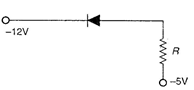
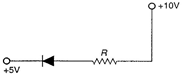
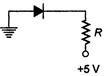
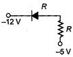
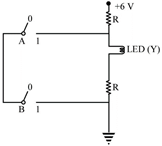
    A zener diode, having breakdown voltage equal to 15 V, is used in a voltage regulator circuit shown in figure. The current through the diode is                                                        [AIPMT (M) 2011]

    A)
     10 mA             

    B)
     15 mA

    C)
          20 mA             

    D)
          5 mA

    View Answer play_arrow
  • question_answer63) 
    Symbolic representation of four logic gates are shown as                  [AIPMT (S) 2011]
    (i)                                 (ii)
    (iii)                                (iv)
    Pick out which ones are for AND, NAND and NOT gates, respectively.

    A)
     (iii), (ii) and (i)  

    B)
          (iii), (ii) and (iv)

    C)
                                                 (ii), (iv) and (iii)

    D)
          (ii), (iii) and (iv)

    View Answer play_arrow
  • question_answer64) If a small amount of antimony is added to germanium crystal                [AIPMT (S) 2011]

    A)
     the antimony becomes an acceptor atom

    B)
     there will be more free electrons than holes in the semiconductor

    C)
     its resistance is increased

    D)
     it becomes a p-type semiconductor

    View Answer play_arrow
  • question_answer65) In forward biasing of the \[p-n\] junction                                                                             [AIPMT (S) 2011]

    A)
     the positive terminal of the battery is connected to n-side and the depletion region becomes thin                  

    B)
     the positive terminal of the battery is connected to n-side and the depletion region becomes thick                  

    C)
     the positive terminal of the battery is connected to p-side and the depletion region become thin                   

    D)
     the positive terminal of the battery is connected to p-side and the depletion region becomes thick                   

    View Answer play_arrow
  • question_answer66) A transistor is operated in common emitter configuration at \[{{V}_{C}}=2\text{ }V\] such that a change in the base current from \[100\,\,\mu A\] to \[300\,\,\mu A\] produces a change in the collector current from 10 mA to 20 mA. The current gain is                                                                                                                        [AIPMT (S) 2011]

    A)
     75          

    B)
     100

    C)
                      25        

    D)
     50

    View Answer play_arrow
  • question_answer67) The input resistance of a silicon transistor is \[100\,\Omega \]. Base current is changed by \[40\,\,\mu A\] which results in a change in collector current by 2 mA. This transistor is used as a common-emitter amplifier with a load resistance of \[4\,\,k\,\Omega \]. The voltage gain of the amplifier is                                                [AIPMT (M) 2012]

    A)
     2000     

    B)
     3000   

    C)
     4000               

    D)
          1000

    View Answer play_arrow
  • question_answer68) 
    To get an output \[Y=1\] in given circuit which of the following input will be correct                 [AIPMT (M) 2012]
                            A          B          C

    A)
    1          0          0

    B)
    1          0          1

    C)
                1          1          0

    D)
                0          1          0

    View Answer play_arrow
  • question_answer69) 
    Two ideal diodes are connected to a battery as shown in the circuit. The current supplied by the battery is                                                                                                                                              [AIPMT (S) 2012]                                        

    A)
     0.75 A      

    B)
     zero                 

    C)
     0.25 A 

    D)
     0.5 A

    View Answer play_arrow
  • question_answer70) In a CE transistor amplifier, the audio signal voltage across the collector resistance of \[2\,k\Omega \] is 2V. If the base resistance is \[1\,k\Omega \] and the current amplification of the transistor is 100, the input signal voltage is                            [AIPMT (S) 2012]

    A)
     0.1 V      

    B)
     1.0 V

    C)
          1 mV    

    D)
      10 Mv

    View Answer play_arrow
  • question_answer71) C and Si both have same lattice structure, having 4 bonding electrons in each. However, C is insulator whereas Si is intrinsic semiconductor. This is because                                                                             [AIPMT (S) 2012]

    A)
     in case of C, the valence band is not completely filled at absolute zero temperature

    B)
     in case of C, the conduction band is partly filled even at absolute zero temperature

    C)
     the four bonding electrons in the case of C  lie in the second orbit, whereas in the case of Si they lie in the third

    D)
     the four bonding electrons in the case of C lie in the third orbit, whereas for Si they lie in the fourth orbit

    View Answer play_arrow
  • question_answer72) 
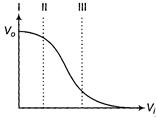
    Transfer characteristic [output voltage \[({{V}_{0}})\] input voltage \[({{V}_{i}})\]] for a base biased transistor in CE configuration is as shown in the figure. For using transistor as a switch, it is used           [AIPMT (S) 2012]
                        

    A)
     in region III

    B)
     both in region (I) and (III)

    C)
     in region II

    D)
     in region I

    View Answer play_arrow
  • question_answer73) 
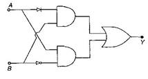
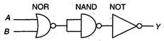
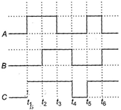
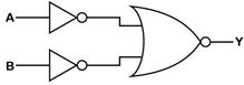
    The figure shows a logic circuit with two inputs A and B and the output C. The voltage wave forms across A, B and C are as given. The logic circuit gate is                                                                                        [AIPMT (S) 2012]

    A)
     OR gate   

    B)
     NOR gate

    C)
          AND gate     

    D)
      NAND gate

    View Answer play_arrow
  • question_answer74) In a n-type semiconductor, which of the following statement is true?                          [NEET 2013]

    A)
     Electrons are majority carriers and trivalent atoms are dopants

    B)
     Electrons are minority carriers and pentavalent atoms are dopants

    C)
     Holes are minority carriers and pentavalen atoms are dopants

    D)
     Holes are majority carriers and trivalent atoms are dopants

    View Answer play_arrow
  • question_answer75) In a common emitter (CE) amplifier having a voltage gain G, the transistor used has trans conductance 0.03 mho and current gain 25. If the above transistor is replaced with another one with trans conductance 0.02 mho and current gain 20, the voltage gain will                                                                                                                         [NEET 2013]

    A)
     \[\frac{2}{3}G\]                       

    B)
     \[1.5\,G\]

    C)
          \[\frac{1}{3}G\]                       

    D)
          \[\frac{5}{4}G\]

    View Answer play_arrow
  • question_answer76) 
    The output (X) of the logic circuit shown in figure will be                                           [NEET 2013]

    A)
     \[X=\overline{\overline{A}}\cdot \overline{\overline{B}}\]

    B)
          \[X=\overline{A\cdot B}\]

    C)
     \[X=A\cdot B\] 

    D)
          \[X=\overline{A+B}\]

    View Answer play_arrow
  • question_answer77) 
    The given graph represents \[V.I\] characteristic for a semiconductor device.              [NEET 2014]
    Which   of   the   following statement is correct?

    A)
     It is \[V-I\] characteristic for solar cell where point A represents open circuit voltage and point B short circuit current

    B)
     It is for a solar cell and points A and B represent open circuit voltage and current, respectively

    C)
     It is for a photodiode and points A and B represent open circuit voltage and current, respectively

    D)
     It is for a LED and points A and B represents open circuit voltage and short circuit current respectively

    View Answer play_arrow
  • question_answer78) 
    The barrier potential of a \[p-n\] junction depends on                                               [NEET 2014]
    (i) type of semiconductor material
    (ii) amount of doping temperature
    (iii) Which one of the following is correct?

    A)
     (i) and (ii) only     

    B)
    (ii) only

    C)
     (ii) and (iii) only 

    D)
    (i), (ii) and (iii)

    View Answer play_arrow
  • question_answer79) 
    If in a \[p-n\] junction, a square input signal of 10 V is applied as shown,
    then the output across \[{{R}_{L}}\] will be                                                                    [NEET  2015]

    A)
     

    B)
                     

    C)
          

    D)
           

    View Answer play_arrow
  • question_answer80)  
    Which logic gate is represented by the following combination of logic gates?                            [NEET  2015]

    A)
     OR                 

    B)
     NAND

    C)
     AND               

    D)
          NOR

    View Answer play_arrow
  • question_answer81) 
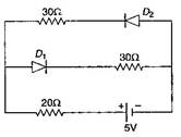
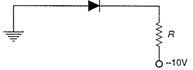
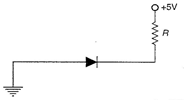
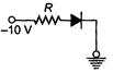
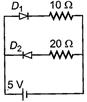
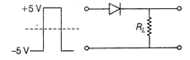
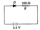
    In the given figure, a diode D is connected to an external resistance \[R=100\,\Omega \] and an, e.m.f of 3.5 V. If the barrier potential developed across the diode is 0.5 V, the current in the circuit will be         [NEET (Re) 2015]

    A)
     30 mA             

    B)
     40 mA

    C)
     20 mA             

    D)
          35 mA

    View Answer play_arrow
  • question_answer82) 
    The input signal given to a CE amplifier having a voltage gain of 150 is
    \[{{V}_{i}}=2\cos \left( 15t+\frac{\pi }{3} \right)\] The corresponding output signal will be    [NEET (Re) 2015]

    A)
     \[300\cos \left( 15t+\frac{\pi }{3} \right)\]

    B)
     \[75\cos \left( 15t+\frac{2\pi }{3} \right)\]

    C)
     \[2\cos \left( 15t+\frac{5\pi }{3} \right)\]

    D)
          \[300\cos \left( 15t+\frac{4\pi }{3} \right)\]

    View Answer play_arrow
  • question_answer83) 
    Consider the junction diode as ideal. The value of current flowing through AB is :                    [NEET - 2016]

    A)
     \[0\,A\]                        

    B)
     \[{{10}^{-2}}A\]

    C)
     \[{{10}^{-1}}A\]        

    D)
     \[{{10}^{-3}}A\]

    View Answer play_arrow
  • question_answer84) A npn transistor is connected in common emitter configuration in a given amplifier. A load resistance of \[800\,\,\Omega \] is connected in the collector circuit and the voltage drop across it is 0.8 V. If the current amplification factor is 0.96 and the input resistance of the circuit is \[192\,\Omega ,\] the voltage gain and the power gain of the amplifier will respectively be :                                                                                                                      [NEET - 2016]

    A)
     4, 3.84            

    B)
          3.69, 3.84

    C)
     4, 4                 

    D)
          4, 3.69

    View Answer play_arrow
  • question_answer85) 
    To get output 1 for the following circuit, the correct choice for the input is                               [NEET - 2016]

    A)
     \[A=0,\text{ }B=1,\text{ }C=0\]

    B)
          \[A=1,\text{ }B=0,\text{ }C=0\]

    C)
      \[A=1,\text{ }B=1,\text{ }C=0\]

    D)
      \[A=1,\text{ }B=0,\text{ }C=1\]

    View Answer play_arrow
  • question_answer86) In a common emitter transistor amplifier the audio signal voltage across the collector is 3 V. The resistance of collector is \[3\,\,k\,\Omega \]. If current gain is 100 and the base resistance is \[2\,\,k\,\Omega ,\] the voltage and power gain of the amplifier is                                                                                                                      [NEET-2017]

    A)
     20 and 2000    

    B)
          200 and 1000

    C)
     15 and 200      

    D)
          150 and 15000

    View Answer play_arrow
  • question_answer87) Which one of the following represents forward bias diode?                             [NEET-2017]

    A)
     

    B)
     

    C)
     

    D)
     

    View Answer play_arrow
  • question_answer88) 
    The given electrical network is equivalent to                                                [NEET-2017]

    A)
     NOT gate         

    B)
          AND gate

    C)
     OR gate           

    D)
          NOR gate

    View Answer play_arrow
  • question_answer89) 
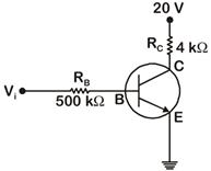
    In the circuit shown in the figure, the input voltage \[{{\text{V}}_{\text{i}}}\] is 20 V, \[{{V}_{BE}}=0\]and\[{{V}_{CE}}=0\]. The values of \[{{\text{I}}_{\text{B}}}\text{,}{{\text{I}}_{\text{C}}}\] and \[\beta \] are given by                                                                                                             [NEET - 2018]

    A)
     \[{{I}_{B}}=20\mu A,{{I}_{C}}=5mA,\beta =250\]

    B)
     \[{{I}_{B}}=25\mu A,{{I}_{C}}=5mA,\beta =200\]

    C)
     \[{{I}_{B}}=40\mu A,\,\,{{I}_{C}}=10mA,\,\,\beta =250\]

    D)
     \[{{I}_{B}}=40\mu A,\,\,{{I}_{C}}=5mA,\,\,\beta =125\]

    View Answer play_arrow
  • question_answer90) In a p-n junction diode, change in temperature due to heating                                  [NEET - 2018]

    A)
     Does not affect resistance of p-n junction

    B)
     Affects only forward resistance

    C)
     Affects only reverse resistance

    D)
     Affects the overall \[\text{V - l}\]characteristics of p-n junction

    View Answer play_arrow
  • question_answer91) 
    In the combination of the following gates the output Y can be written in terms of inputs A and B as                                                                                                                    [NEET - 2018]

    A)
     \[\overline{\text{A}\cdot \text{B}}+\text{A}\cdot \text{B}\]

    B)
          \[\text{A}\cdot \overline{\text{B}}+\overline{\text{A}}\cdot \text{B}\]

    C)
     \[\overline{\text{A}\cdot \text{B}}\]       

    D)
          \[\overline{\text{A+B}}\]

    View Answer play_arrow
  • question_answer92) 
    The correct Boolean operation represented by the circuit diagram drawn is:              [NEET 2019]

    A)
     NAND

    B)
          NOR

    C)
     AND   

    D)
          OR

    View Answer play_arrow
  • question_answer93) For a p-type semiconductor, which of the following statements is true?        [NEET 2019]

    A)
     Holes are the majority carriers and pentavalent atoms are the dopants

    B)
     Electrons are the majority carriers and pentavalent atoms are the dopants

    C)
     Electrons are the majority carriers and trivalent atoms are teh dopants

    D)
     Holes are the majority carriers and trivalent atoms are the dopants

    View Answer play_arrow
  • question_answer94) The increase in the width of the depletion region in a p-n junction diode is due to:        [NEET 2020]

    A)
     reverse bias only

    B)
     both forward bias and reverse bias

    C)
     increase in forward current

    D)
     forward bias only

    View Answer play_arrow
  • question_answer95) For transistor action, which of the following statements is correct?                                          [NEET 2020]

    A)
     Base, emitter and collector regions should have same size.

    B)
     Both emitter junction as well as the collector junction are forward biased.

    C)
     The base region must be very thin and lightly doped.

    D)
     Base, emitter and collector regions should have same doping concentrations.

    View Answer play_arrow
  • question_answer96) 
    For the logic circuit shown, the truth table is:
                                                                                                                                       [NEET 2020]

    A)
                            A          B          Y             0          0          0                         0          1          1                         1          0          1 1          1          1

    B)
                A          B          Y                         0          0          1                         0          1          1                         1          0          1                         1          1          0

    C)
                A          B          Y                         0          0          1                         0          1          0                         1          0          0                                  1          1          0

    D)
                A          B          Y                         0          0          0                         0          1          0                         1          0          0                         1          1          1

    View Answer play_arrow

Study Package

NEET PYQ-Semiconducting Devices


You need to login to perform this action.
You will be redirected in 3 sec spinner