-
question_answer1)
The majority charge carriers in P-type semiconductor are [MP PMT 1999; CBSE PMT 1999; MP PET 1991; MP PET/PMT 1998; MH CET 2003]
A)
Electrons done
clear
B)
Protons done
clear
C)
Holes done
clear
D)
Neutrons done
clear
View Solution play_arrow
-
question_answer2)
A P-type semiconductor can be obtained by adding [NCERT 1979; BIT 1988; MP PMT 1987; 90]
A)
Arsenic to pure silicon done
clear
B)
Gallium to pure silicon done
clear
C)
Antimony to pure germanium done
clear
D)
Phosphorous to pure germanium done
clear
View Solution play_arrow
-
question_answer3)
The valence of an impurity added to germanium crystal in order to convert it into a P-type semi conductor is [MP PMT 1989; CPMT 1987]
A)
6 done
clear
B)
5 done
clear
C)
4 done
clear
D)
3 done
clear
View Solution play_arrow
-
question_answer4)
In a semiconductor, the concentration of electrons is \[8\times {{10}^{14}}/c{{m}^{3}}\]and that of the holes is \[5\times {{10}^{12}}c{{m}^{3}}.\] The semiconductor is [MP PMT 1997; RPET 1999; Kerala PET 2002]
A)
P-type done
clear
B)
N-type done
clear
C)
Intrinsic done
clear
D)
PNP-type done
clear
View Solution play_arrow
-
question_answer5)
In P-type semiconductor, there is [MP PMT 1989]
A)
An excess of one electron done
clear
B)
Absence of one electron done
clear
C)
A missing atom done
clear
D)
A donar level done
clear
View Solution play_arrow
-
question_answer6)
The valence of the impurity atom that is to be added to germanium crystal so as to make it a N-type semiconductor, is [MNR 1993; MP PET 1994; CBSE PMT 1999; AIIMS 2000]
A)
6 done
clear
B)
5 done
clear
C)
4 done
clear
D)
3 done
clear
View Solution play_arrow
-
question_answer7)
Silicon is a semiconductor. If a small amount of As is added to it, then its electrical conductivity [MP PMT 1996]
A)
Decreases done
clear
B)
Increases done
clear
C)
Remains unchanged done
clear
D)
Becomes zero done
clear
View Solution play_arrow
-
question_answer8)
When the electrical conductivity of a semi- conductor is due to the breaking of its covalent bonds, then the semiconductor is said to be [AIIMS 1997; KCET (Engg.) 2002]
A)
Donar done
clear
B)
Acceptor done
clear
C)
Intrinsic done
clear
D)
Extrinsic done
clear
View Solution play_arrow
-
question_answer9)
A piece of copper and the other of germanium are cooled from the room temperature to 80 K, then which of the following would be a correct statement [IIT-JEE 1988; Bihar CEE 1992; CBSE PMT 1993; MP PET 1997; RPET 1999; AIEEE 2004]
A)
Resistance of each increases done
clear
B)
Resistance of each decreases done
clear
C)
Resistance of copper increases while that of germanium decreases done
clear
D)
Resistance of copper decreases while that of germanium increases done
clear
View Solution play_arrow
-
question_answer10)
To obtain P-type \[Si\] semiconductor, we need to dope pure \[Si\] with [IIT-JEE 1988; MP PET 1997, 93; Pb. PMT 2001, 02; UPSEAT 2004]
A)
Aluminium done
clear
B)
Phosphorous done
clear
C)
Oxygen done
clear
D)
Germanium done
clear
View Solution play_arrow
-
question_answer11)
Electrical conductivity of a semiconductor [MP PMT 1993, 2000; RPET 1996]
A)
Decreases with the rise in its temperature done
clear
B)
Increases with the rise in its temperature done
clear
C)
Does not change with the rise in its temperature done
clear
D)
First increases and then decreases with the rise in its temperature done
clear
View Solution play_arrow
-
question_answer12)
Three semi-conductors are arranged in the increasing order of their energy gap as follows. The correct arrangement is [MP PMT 1993]
A)
Tellurium, germanium, silicon done
clear
B)
Tellurium, silicon, germanium done
clear
C)
Silicon, germanium, tellurium done
clear
D)
Silicon, tellurium, germanium done
clear
View Solution play_arrow
-
question_answer13)
When a semiconductor is heated, its resistance [KCET 1992; MP PMT 1994; MP PET 1992, 2002; RPMT 2001; DCE 2001]
A)
Decreases done
clear
B)
Increases done
clear
C)
Remains unchanged done
clear
D)
Nothing is definite done
clear
View Solution play_arrow
-
question_answer14)
In an insulator, the forbidden energy gap between the valence band and conduction band is of the order of [DPMT 1988; EAMCET (Engg.) 1995; MP PET 1996]
A)
\[1\,MeV\] done
clear
B)
\[0.1\,MeV\] done
clear
C)
\[1\,eV\] done
clear
D)
\[5\,eV\] done
clear
View Solution play_arrow
-
question_answer15)
A N-type semiconductor is [AFMC 1988; RPMT 1999]
A)
Negatively charged done
clear
B)
Positively charged done
clear
C)
Neutral done
clear
D)
None of these done
clear
View Solution play_arrow
-
question_answer16)
The energy band gap of \[Si\] is [MP PET 1994, 2002; BHU 1995; RPMT 2000]
A)
\[0.70\,eV\] done
clear
B)
1.1 eV done
clear
C)
Between \[0.70\,eV\] to \[1.1\,eV\] done
clear
D)
5 eV done
clear
View Solution play_arrow
-
question_answer17)
The forbidden energy band gap in conductors, semiconductors and insulators are \[E{{G}_{1}},\,E{{G}_{2}}\]and \[E{{G}_{3}}\] respectively. The relation among them is [MP PMT 1994; RPMT 1997]
A)
\[E{{G}_{1}}=E{{G}_{2}}=E{{G}_{3}}\] done
clear
B)
\[E{{G}_{1}}<E{{G}_{2}}<E{{G}_{3}}\] done
clear
C)
\[E{{G}_{1}}>E{{G}_{2}}>E{{G}_{3}}\] done
clear
D)
\[E{{G}_{1}}<E{{G}_{2}}>E{{G}_{3}}\] done
clear
View Solution play_arrow
-
question_answer18)
Which statement is correct [MP PMT 1994]
A)
N-type germanium is negatively charged and P-type germanium is positively charged done
clear
B)
Both N-type and P-type germanium are neutral done
clear
C)
N-type germanium is positively charged and P-type germanium is negatively charged done
clear
D)
Both N-type and P-type germanium are negatively charged done
clear
View Solution play_arrow
-
question_answer19)
When Ge crystals are doped with phosphorus atom, then it becomes [AFMC 1995; Orissa PMT 2004]
A)
Insulator done
clear
B)
P-type done
clear
C)
N-type done
clear
D)
Superconductor done
clear
View Solution play_arrow
-
question_answer20)
Let \[{{n}_{P}}\] and \[{{n}_{e}}\] be the number of holes and conduction electrons respectively in a semiconductor. Then [MP PET 1995]
A)
\[{{n}_{P}}>{{n}_{e}}\]in an intrinsic semiconductor done
clear
B)
\[{{n}_{P}}={{n}_{e}}\]in an extrinsic semiconductor done
clear
C)
\[{{n}_{P}}={{n}_{e}}\]in an intrinsic semiconductor done
clear
D)
\[{{n}_{e}}>{{n}_{P}}\]in an intrinsic semiconductor done
clear
View Solution play_arrow
-
question_answer21)
Wires P and Q have the same resistance at ordinary (room) temperature. When heated, resistance of \[P\] increases and that of Q decreases. We conclude that [MP PMT 1995; MP PET 2001]
A)
P and Q are conductors of different materials done
clear
B)
P is N-type semiconductor and Q is P-type semiconductor done
clear
C)
P is semiconductor and Q is conductor done
clear
D)
P is conductor and Q is semiconductor done
clear
View Solution play_arrow
-
question_answer22)
The impurity atoms which are mixed with pure silicon to make a P-type semiconductor are those of [MP PMT 1995]
A)
Phosphorus done
clear
B)
Boron done
clear
C)
Antimony done
clear
D)
Copper done
clear
View Solution play_arrow
-
question_answer23)
Holes are charge carriers in [IIT-JEE 1996]
A)
Intrinsic semiconductors done
clear
B)
Ionic solids done
clear
C)
P-type semiconductors done
clear
D)
Metals done
clear
View Solution play_arrow
-
question_answer24)
In extrinsic P and N-type, semiconductor materials, the ratio of the impurity atoms to the pure semiconductor atoms is about [MP PET 2003]
A)
1 done
clear
B)
\[{{10}^{-1}}\] done
clear
C)
\[{{10}^{-4}}\] done
clear
D)
\[{{10}^{-7}}\] done
clear
View Solution play_arrow
-
question_answer25)
A hole in a P-type semiconductor is [MP PET 1996]
A)
An excess electron done
clear
B)
A missing electron done
clear
C)
A missing atom done
clear
D)
A donor level done
clear
View Solution play_arrow
-
question_answer26)
The forbidden gap in the energy bands of germanium at room temperature is about [MP PMT/PET 1998]
A)
\[1.1eV\] done
clear
B)
\[0.1eV\] done
clear
C)
\[0.67eV\] done
clear
D)
\[6.7eV\] done
clear
View Solution play_arrow
-
question_answer27)
In P-type semiconductor the majority and minority charge carriers are respectively [EAMCET 1994; MP PMT/PET 1998; MH CET 2000]
A)
Protons and electrons done
clear
B)
Electrons and protons done
clear
C)
Electrons and holes done
clear
D)
Holes and electrons done
clear
View Solution play_arrow
-
question_answer28)
At zero Kelvin a piece of germanium [MP PET 1999]
A)
Becomes semiconductor done
clear
B)
Becomes good conductor done
clear
C)
Becomes bad conductor done
clear
D)
Has maximum conductivity done
clear
View Solution play_arrow
-
question_answer29)
Electronic configuration of germanium is 2, 8, 18 and 4. To make it extrinsic semiconductor small quantity of antimony is added [MP PET 1999]
A)
The material obtained will be N-type germanium in which electrons and holes are equal in number done
clear
B)
The material obtained will be P-type germanium done
clear
C)
The material obtained will be N-type germanium which has more electrons than holes at room temperature done
clear
D)
The material obtained will be N-type germanium which has less electrons than holes at room temperature done
clear
View Solution play_arrow
-
question_answer30)
A semiconductor is cooled from \[{{T}_{1}}K\] to \[{{T}_{2}}K.\] Its resistance [MP PET 1999]
A)
Will decrease done
clear
B)
Will increase done
clear
C)
Will first decrease and then increase done
clear
D)
Will not change done
clear
View Solution play_arrow
-
question_answer31)
If \[{{N}_{P}}\]and \[{{N}_{e}}\]be the numbers of holes and conduction electrons in an extrinsic semiconductor, then [MP PMT 1999; AMU 2001]
A)
\[{{N}_{P}}>{{N}_{e}}\] done
clear
B)
\[{{N}_{P}}={{N}_{e}}\] done
clear
C)
\[{{N}_{P}}<{{N}_{e}}\] done
clear
D)
\[{{N}_{P}}>{{N}_{e}}\] or \[{{N}_{P}}<{{N}_{e}}\] depending on the nature of impurity done
clear
View Solution play_arrow
-
question_answer32)
In intrinsic semiconductor at room temperature, number of electrons and holes are [EAMCET (Engg.) 1995; JIPMER 2001, 02]
A)
Equal done
clear
B)
Zero done
clear
C)
Unequal done
clear
D)
Infinite done
clear
View Solution play_arrow
-
question_answer33)
(USS 133) Indium impurity in germanium makes [EAMCET (Engg.) 1995]
A)
N-type done
clear
B)
P-type done
clear
C)
Insulator done
clear
D)
Intrinsic done
clear
View Solution play_arrow
-
question_answer34)
Fermi level of energy of an intrinsic semiconductor lies [EAMCET (Med.) 1995]
A)
In the middle of forbidden gap done
clear
B)
Below the middle of forbidden gap done
clear
C)
Above the middle of forbidden gap done
clear
D)
Outside the forbidden gap done
clear
View Solution play_arrow
-
question_answer35)
In a semiconductor the separation between conduction band and valence band is of the order of [EAMCET (Med.) 1995; AIIMS 2000]
A)
\[100\,eV\] done
clear
B)
\[10\,eV\] done
clear
C)
\[1\,eV\] done
clear
D)
0 eV done
clear
View Solution play_arrow
-
question_answer36)
The intrinsic semiconductor becomes an insulator at [EAMCET (Med.) 1995; KCET (Engg./Med.) 1999; MP PET 2000; CBSE PMT 2001]
A)
\[0{}^\circ C\] done
clear
B)
\[-100{}^\circ C\] done
clear
C)
\[300\ K\] done
clear
D)
\[0\ K\] done
clear
View Solution play_arrow
-
question_answer37)
The addition of antimony atoms to a sample of intrinsic germanium transforms it to a material which is [AMU 1995]
A)
Superconductor done
clear
B)
An insulator done
clear
C)
N-type semiconductor done
clear
D)
P-type semiconductor done
clear
View Solution play_arrow
-
question_answer38)
Resistance of semiconductor at \[0{}^\circ K\] is [RPET 1997]
A)
Zero done
clear
B)
Infinite done
clear
C)
Large done
clear
D)
Small done
clear
View Solution play_arrow
-
question_answer39)
In a good conductor the energy gap between the conduction band and the valence band is [KCET 1993; EMCET (Med.) 1994]
A)
Infinite done
clear
B)
Wide done
clear
C)
Narrow done
clear
D)
Zero done
clear
View Solution play_arrow
-
question_answer40)
The impurity atom added to germanium to make it N-type semiconductor is [KCET 1993; KCET (Engg./Med.) 2000]
A)
Arsenic done
clear
B)
Iridium done
clear
C)
Aluminium done
clear
D)
Iodine done
clear
View Solution play_arrow
-
question_answer41)
When N-type of semiconductor is heated [CBSE PMT 1993; DPMT 2000]
A)
Number of electrons increases while that of holes decreases done
clear
B)
Number of holes increases while that of electrons decreases done
clear
C)
Number of electrons and holes remains same done
clear
D)
Number of electrons and holes increases equally done
clear
View Solution play_arrow
-
question_answer42)
To obtain a P-type germanium semiconductor, it must be doped with [CBSE PMT 1997; Pb. PET 2000]
A)
Arsenic done
clear
B)
Antimony done
clear
C)
Indium done
clear
D)
Phosphorus done
clear
View Solution play_arrow
-
question_answer43)
The temperature coefficient of resistance of a semiconductor [AFMC 1998, MNR 1998]
A)
Is always positive done
clear
B)
Is always negative done
clear
C)
Is zero done
clear
D)
May be positive or negative or zero done
clear
View Solution play_arrow
-
question_answer44)
P-type semiconductor is formed when [RPET 1999] A. As impurity is mixed in Si B. Al impurity is mixed in Si C. B impurity is mixed in Ge D. P impurity is mixed in Ge
A)
A and C done
clear
B)
A and D done
clear
C)
B and C done
clear
D)
B and D done
clear
View Solution play_arrow
-
question_answer45)
In case of a semiconductor, which of the following statement is wrong [Pb. PMT 1999]
A)
Doping increases conductivity done
clear
B)
Temperature coefficient of resistance is negative done
clear
C)
Resisitivity is in between that of a conductor and insulator done
clear
D)
At absolute zero temperature, it behaves like a conductor done
clear
View Solution play_arrow
-
question_answer46)
Energy bands in solids are a consequence of [DCE 1999, 2000; AIEEE 2004]
A)
Ohm?s Law done
clear
B)
Pauli?s exclusion principle done
clear
C)
Bohr?s theory done
clear
D)
Heisenberg?s uncertainty principle done
clear
View Solution play_arrow
-
question_answer47)
In a P-type semiconductor [AIIMS 1997; Orissa JEE 2002; MP PET 2003]
A)
Current is mainly carried by holes done
clear
B)
Current is mainly carried by electrons done
clear
C)
The material is always positively charged done
clear
D)
Doping is done by pentavalent material done
clear
View Solution play_arrow
-
question_answer48)
At ordinary temperatures, the electrical conductivity of semi conductors in \[mho/mete\text{r}\] is in the range [MP PET 2003]
A)
\[{{10}^{-3}}\] to \[{{10}^{-4}}\] done
clear
B)
\[{{10}^{6}}\text{ to }{{10}^{9}}\] to \[{{10}^{9}}\] done
clear
C)
\[{{10}^{-6}}\] to \[{{10}^{-10}}\] done
clear
D)
\[{{10}^{-10}}\] to \[{{10}^{-16}}\] done
clear
View Solution play_arrow
-
question_answer49)
When the temperature of silicon sample is increased from \[27{}^\circ C\] to \[100{}^\circ C\], the conductivity of silicon will be [RPMT 1999]
A)
Increased done
clear
B)
Decreased done
clear
C)
Remain same done
clear
D)
Zero done
clear
View Solution play_arrow
-
question_answer50)
In a P-type semiconductor, germanium is doped with [AFMC 1999]
A)
Boron done
clear
B)
Gallium done
clear
C)
Aluminium done
clear
D)
All of these done
clear
View Solution play_arrow
-
question_answer51)
In N-type semiconductors, majority charge carriers are [AIIMS 1999]
A)
Holes done
clear
B)
Protons done
clear
C)
Neutrons done
clear
D)
Electrons done
clear
View Solution play_arrow
-
question_answer52)
Semiconductor is damaged by the strong current due to [MH CET 2000]
A)
Lack of free electron done
clear
B)
Excess of electrons done
clear
C)
Excess of proton done
clear
D)
None of these done
clear
View Solution play_arrow
-
question_answer53)
GaAs is [RPMT 2000]
A)
Element semiconductor done
clear
B)
Alloy semiconductor done
clear
C)
Bad conductor done
clear
D)
Metallic semiconductor done
clear
View Solution play_arrow
-
question_answer54)
If \[{{n}_{e}}\] and \[{{n}_{h}}\] are the number of electrons and holes in a semiconductor heavily doped with phosphorus, then [MP PMT 2000]
A)
\[{{n}_{e}}>>{{n}_{h}}\] done
clear
B)
\[{{n}_{e}}<<{{n}_{h}}\] done
clear
C)
\[{{n}_{e}}\le {{n}_{h}}\] done
clear
D)
\[{{n}_{e}}={{n}_{h}}\] done
clear
View Solution play_arrow
-
question_answer55)
An N-type and P-type silicon can be obtained by doping pure silicon with [EAMCET (Med.) 2000]
A)
Arsenic and Phosphorous done
clear
B)
Indium and Aluminium done
clear
C)
Phosphorous and Indium done
clear
D)
Aluminium and Boron done
clear
View Solution play_arrow
-
question_answer56)
N-type semiconductors will be obtained, when germanium is doped with [AIIMS 2000]
A)
Phosphorus done
clear
B)
Aluminium done
clear
C)
Arsenic done
clear
D)
Both (a) or (c) done
clear
View Solution play_arrow
-
question_answer57)
The state of the energy gained by valance electrons when the temperature is raised or when electric field is applied is called as [CBSE PMT 2000]
A)
Valance band done
clear
B)
Conduction band done
clear
C)
Forbidden band done
clear
D)
None of these done
clear
View Solution play_arrow
-
question_answer58)
To obtain electrons as majority charge carriers in a semiconductor, the impurity mixed is [MP PET 2000]
A)
Monovalent done
clear
B)
Divalent done
clear
C)
Trivalent done
clear
D)
Pentavalent done
clear
View Solution play_arrow
-
question_answer59)
For germanium crystal, the forbidden energy gap in joules is [MP PET 2000]
A)
\[1.12\times {{10}^{-19}}\] done
clear
B)
\[1.76\times {{10}^{-19}}\] done
clear
C)
\[1.6\times {{10}^{-19}}\] done
clear
D)
Zero done
clear
View Solution play_arrow
-
question_answer60)
A pure semiconductor behaves slightly as a conductor at [MH CET (Med.) 2001; BHU 2000; AFMC 2001]
A)
Room temperature done
clear
B)
Low temperature done
clear
C)
High temperature done
clear
D)
Both (b) and (c) done
clear
View Solution play_arrow
-
question_answer61)
Which is the correct relation for forbidden energy gap in conductor, semi conductor and insulator [RPMT 2001; AIEEE 2002]
A)
\[\Delta E{{g}_{\text{c}}}>\Delta E{{g}_{\text{sc}}}>\Delta E{{g}_{\text{insulator}}}\] done
clear
B)
\[\Delta E{{g}_{\text{insulator}}}>\Delta E{{g}_{\text{sc}}}>\Delta E{{g}_{\text{conductor}}}\] done
clear
C)
\[\Delta E{{g}_{\text{conductor}}}>\Delta E{{g}_{\text{insulator}}}>\Delta E{{g}_{\text{sc}}}\] done
clear
D)
\[\Delta E{{g}_{\text{sc}}}>\Delta E{{g}_{\text{conductor}}}>\Delta E{{g}_{\text{insulator}}}\] done
clear
View Solution play_arrow
-
question_answer62)
The band gap in Germanium and silicon in eV respectively is [MP PMT 2001]
A)
0.7, 1.1 done
clear
B)
1.1, 0.7 done
clear
C)
1.1, 0 done
clear
D)
0, 1.1 done
clear
View Solution play_arrow
-
question_answer63)
P-type semiconductors are made by adding impurity element [MP PMT 2001]
A)
As done
clear
B)
P done
clear
C)
B done
clear
D)
Bi done
clear
View Solution play_arrow
-
question_answer64)
At room temperature, a P-type semiconductor has [Kerala PMT 2002]
A)
Large number of holes and few electrons done
clear
B)
Large number of free electrons and few holes done
clear
C)
Equal number of free electrons and holes done
clear
D)
No electrons or holes done
clear
View Solution play_arrow
-
question_answer65)
In intrinsic semiconductor at room temperature, number of electrons and holes are [JIPMER 2001, 02; MP PMT 2002]
A)
Unequal done
clear
B)
Equal done
clear
C)
Infinite done
clear
D)
Zero done
clear
View Solution play_arrow
-
question_answer66)
The valence band and conduction band of a solid overlap at low temperature, the solid may be [Orissa JEE 2002; BCECE 2004]
A)
A metal done
clear
B)
A semiconductor done
clear
C)
An insulator done
clear
D)
None of these done
clear
View Solution play_arrow
-
question_answer67)
Which impurity is doped in Si to form N-type semi-conductor? [CBSE PMT 1996; AIEEE 2002]
A)
Al done
clear
B)
B done
clear
C)
As done
clear
D)
None of these done
clear
View Solution play_arrow
-
question_answer68)
In a semiconductor [AIEEE 2002; AIIMS 2002]
A)
There are no free electrons at any temperature done
clear
B)
The number of free electrons is more than that in a conductor done
clear
C)
There are no free electrons at 0 K done
clear
D)
None of these done
clear
View Solution play_arrow
-
question_answer69)
The energy band gap is maximum in [AIEEE 2002]
A)
Metals done
clear
B)
Superconductors done
clear
C)
Insulators done
clear
D)
Semiconductors done
clear
View Solution play_arrow
-
question_answer70)
The process of adding impurities to the pure semiconductor is called [MH CET 2002]
A)
Drouping done
clear
B)
Drooping done
clear
C)
Doping done
clear
D)
None of these done
clear
View Solution play_arrow
-
question_answer71)
When phosphorus and antimony are mixed in zermaniun, then [CPMT 2003]
A)
P-type semiconductor is formed done
clear
B)
N-type semiconductor is formed done
clear
C)
Both (a) and (b) done
clear
D)
None of these done
clear
View Solution play_arrow
-
question_answer72)
To a germanium sample, traces of gallium are added as an impurity. The resultant sample would behave like [AIIMS 2003]
A)
A conductor done
clear
B)
A P-type semiconductor done
clear
C)
An N-type semiconductor done
clear
D)
An insulator done
clear
View Solution play_arrow
-
question_answer73)
For non-conductors, the energy gap is [EAMCET (Engg.) 1995; MP PET 1996; RPET 2003]
A)
6 eV done
clear
B)
1.1 eV done
clear
C)
0.8 eV done
clear
D)
0.3 eV done
clear
View Solution play_arrow
-
question_answer74)
Donor type impurity is found in [RPET 2003]
A)
Trivalent elements done
clear
B)
Pentavalent elements done
clear
C)
In both the above done
clear
D)
None of these done
clear
View Solution play_arrow
-
question_answer75)
The difference in the variation of resistance with temperature in a metal and a semiconductor arises essentially due to the difference in the [AIEEE 2003]
A)
Variation of scattering mechanism with temperature done
clear
B)
Crystal structure done
clear
C)
Variation of the number of charge carriers with temperature done
clear
D)
Type of bon done
clear
View Solution play_arrow
-
question_answer76)
The charge on a hole is equal to the charge of [MP PMT 2004]
A)
Zero done
clear
B)
Proton done
clear
C)
Neutron done
clear
D)
Electron done
clear
View Solution play_arrow
-
question_answer77)
When germanium is doped with phosphorus, the doped material has [MP PMT 2004]
A)
Excess positive charge done
clear
B)
Excess negative charge done
clear
C)
More negative current carriers done
clear
D)
More positive current carriers done
clear
View Solution play_arrow
-
question_answer78)
A Ge specimen is doped with Al. The concentration of acceptor atoms is ~1021 atoms/m3. Given that the intrinsic concentration of electron hole pairs is \[\tilde{\ }{{10}^{19}}/{{m}^{3}}\], the concentration of electrons in the specimen is [AIIMS 2004]
A)
\[{{10}^{17}}/{{m}^{3}}\] done
clear
B)
\[{{10}^{15}}/{{m}^{3}}\] done
clear
C)
\[{{10}^{4}}/{{m}^{3}}\] done
clear
D)
\[{{10}^{2}}/{{m}^{3}}\] done
clear
View Solution play_arrow
-
question_answer79)
Which of the following has negative temperature coefficient of resistance [AFMC 2004]
A)
Copper done
clear
B)
Aluminium done
clear
C)
Iron done
clear
D)
Germanium done
clear
View Solution play_arrow
-
question_answer80)
In semiconductors at a room temperature [CBSE PMT 2004]
A)
The valence band is partially empty and the conduction band is partially filled done
clear
B)
The valence band is completely filled and the conduction band is partially filled done
clear
C)
The valence band is completely filled done
clear
D)
The conduction band is completely empty done
clear
View Solution play_arrow
-
question_answer81)
Regarding a semiconductor which one of the following is wrong [CPMT 2004]
A)
There are no free electrons at room temperature done
clear
B)
There are no free electrons at 0 K done
clear
C)
The number of free electrons increases with rise of temperature done
clear
D)
The charge carriers are electrons and holes done
clear
View Solution play_arrow
-
question_answer82)
Which of the following statements is true for an N-type semi-conductor [CPMT 2004]
A)
The donor level lies closely below the bottom of the conduction band done
clear
B)
The donor level lies closely above the top of the valence band done
clear
C)
The donor level lies at the halfway mark of the forbidden energy gap done
clear
D)
None of above done
clear
View Solution play_arrow
-
question_answer83)
Choose the correct statement [DCE 2004]
A)
When we heat a semiconductor its resistance increases done
clear
B)
When we heat a semiconductor its resistance decreases done
clear
C)
When we cool a semiconductor to 0 K then it becomes super conductor done
clear
D)
Resistance of a semiconductor is independent of temperature done
clear
View Solution play_arrow
-
question_answer84)
In a P-type semi-conductor, germanium is dopped with [MH CET 2003]
A)
Gallium done
clear
B)
Boron done
clear
C)
Aluminium done
clear
D)
All of these done
clear
View Solution play_arrow
-
question_answer85)
A piece of semiconductor is connected in series in an electric circuit. On increasing the temperature, the current in the circuit will [RPMT 2003]
A)
Decrease done
clear
B)
Remain unchanged done
clear
C)
Increase done
clear
D)
Stop flowing done
clear
View Solution play_arrow
-
question_answer86)
Intrinsic semiconductor is electrically neutral. Extrinsic semiconductor having large number of current carriers would be [AMU (Engg.) 2001]
A)
Positively charged done
clear
B)
Negatively charged done
clear
C)
Positively charged or negatively charged depending upon the type of impurity that has been added done
clear
D)
Electrically neutral done
clear
View Solution play_arrow
-
question_answer87)
If ne and vd be the number of electrons and drift velocity in a semiconductor. When the temperature is increased [Pb. CET 2000]
A)
ne increases and vd decreases done
clear
B)
ne decreases and vd increases done
clear
C)
Both ne and vd increases done
clear
D)
Both ne and vd decreases done
clear
View Solution play_arrow
-
question_answer88)
In extrinsic semiconductors [EAMCET (Engg.) 1999]
A)
The conduction band and valence band overlap done
clear
B)
The gap between conduction band and valence band is more than 16 eV done
clear
C)
The gap between conduction band and valence band is near about 1 eV done
clear
D)
The gap between conduction band and valence band will be 100 eV and more done
clear
View Solution play_arrow
-
question_answer89)
Resistivity of a semiconductor depends on [MP PMT 1999]
A)
Shape of semiconductor done
clear
B)
Atomic nature of semiconductor done
clear
C)
Length of semiconductor done
clear
D)
Shape and atomic nature of semiconductor done
clear
View Solution play_arrow
-
question_answer90)
Electric current is due to drift of electrons in [CPMT 1996]
A)
Metallic conductors done
clear
B)
Semi-conductors done
clear
C)
Both (a) and (b) done
clear
D)
None of these done
clear
View Solution play_arrow
-
question_answer91)
The energy gap of silicon is 1.14 eV. The maximum wavelength at which silicon will begin absorbing energy is [MP PMT 1993]
A)
10888 Å done
clear
B)
1088.8 Å done
clear
C)
108.88 Å done
clear
D)
10.888 Å done
clear
View Solution play_arrow
-
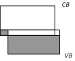
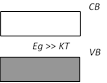
question_answer92)
Which of the following energy band diagram shows the N-type semiconductor [RPET 1986]
A)
B)
C)
D)
View Solution play_arrow
-
question_answer93)
The mobility of free electron is greater than that of free holes because
A)
The carry negative charge done
clear
B)
They are light done
clear
C)
They mutually collide less done
clear
D)
They require low energy to continue their motion done
clear
View Solution play_arrow
-
question_answer94)
The relation between the number of free electrons in semiconductors (n) and its temperature (T) is
A)
\[n\propto {{T}^{2}}\] done
clear
B)
\[n\propto T\] done
clear
C)
\[n\propto \sqrt{T}\] done
clear
D)
\[n\propto {{T}^{3/2}}\] done
clear
View Solution play_arrow
-
question_answer95)
The electron mobility in N-type germanium is 3900 cm2/v-s and its conductivity is 6.24 mho/cm, then impurity concentration will be if the effect of cotters is negligible
A)
1015 cm3 done
clear
B)
1013 /cm3 done
clear
C)
1012 /cm3 done
clear
D)
1016 /cm3 done
clear
View Solution play_arrow
-
question_answer96)
Which of the energy band diagrams shown in the figure corresponds to that of a semiconductor [Orissa JEE 2003]
A)
B)
C)
D)
View Solution play_arrow
-
question_answer97)
The energy band diagrams for three semiconductor samples of silicon are as shown. We can then assert that [Haryana CEE 1996]
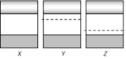
A)
Sample X is undoped while samples Y and Z have been doped with a third group and a fifth group impurity respectively done
clear
B)
Sample X is undoped while both samples Y and Z have been doped with a fifth group impurity done
clear
C)
Sample X has been doped with equal amounts of third and fifth group impurities while samples Y and Z are undoped done
clear
D)
Sample X is undoped while samples Y and Z have been doped with a fifth group and a third group impurity respectively done
clear
View Solution play_arrow
-
question_answer98)
Carbon, silicon and Germanium atoms have four valence electrons each. Their valence and conduction band are separated by energy band gaps represented by (Eg)C. (Eg)Si and (Eg)Ge respectively. Which one of the following relationship is true in their case [CBSE PMT 2005]
A)
\[{{({{E}_{g}})}_{C}}>{{({{E}_{g}})}_{Si}}\] done
clear
B)
\[{{({{E}_{g}})}_{C}}={{({{E}_{g}})}_{Si}}\] done
clear
C)
\[{{({{E}_{g}})}_{C}}<{{({{E}_{g}})}_{Ge}}\] done
clear
D)
\[{{({{E}_{g}})}_{C}}<{{({{E}_{g}})}_{Si}}\] done
clear
View Solution play_arrow
-
question_answer99)
A semiconductor dopped with a donor impurity is [AFMC 2005]
A)
P-type done
clear
B)
N-type done
clear
C)
NPN type done
clear
D)
PNP type done
clear
View Solution play_arrow
-
question_answer100)
In a semiconducting material the mobilities of electrons and holes are me and mh respectively. Which of the following is true [AIIMS 2005]
A)
\[{{\mu }_{e}}>{{\mu }_{h}}\] done
clear
B)
\[{{\mu }_{e}}<{{\mu }_{h}}\] done
clear
C)
\[{{\mu }_{e}}={{\mu }_{h}}\] done
clear
D)
\[{{\mu }_{e}}<0;\ {{\mu }_{h}}>0\] done
clear
View Solution play_arrow
-
question_answer101)
Doping of intrinsic semiconductor is done [Orissa JEE 2005]
A)
To neutralize charge carriers done
clear
B)
To increase the concentration of majority charge carriers done
clear
C)
To make it neutral before disposal done
clear
D)
To carry out further purification done
clear
View Solution play_arrow
 done
clear
done
clear
 done
clear
done
clear
 done
clear
done
clear
 done
clear
done
clear
 done
clear
done
clear
 done
clear
done
clear
 done
clear
done
clear
 done
clear
done
clear


