| (i) Using the necessary circuit diagram, draw the transfer characteristics of a base-biased transistor in CE configuration. With the help of these characteristics, explain briefly how the transistor can be used as an amplifier. |
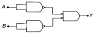
| (ii) Why are NAND gate called universal gates? Identify the logic operations carried out by the circuit shown below |
 |
| Logic circuit |
| Or |
| (i) Draw a circuit diagram to study the input and output characteristics of an n-p-n transistor in its common emitter configuration. Draw the typical input and output characteristics. |
| (ii) Explain, with the help of a circuit diagram, the working of n-p-n transistor as a common emitter amplifier. |
Answer:
(i) Circuit diagram A base biased n-p-n transistor in CE configuration. 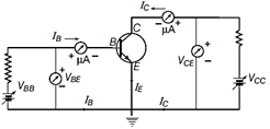 Transfer characteristics
 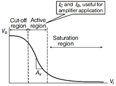 Transfer characteristics of base biased CE transistor. The active region of a transfer characteristics curve can be used to explain the transistor as an amplifier. The resistance of output circuit is large being in reverse bias and resistance of input circuit is low being in forward bias. When input voltage, \[{{V}_{BE}}\]comes in active region,\[{{I}_{C}}\] flows in output and \[{{V}_{O}}\]varies significantly as \[{{V}_{O}}={{V}_{CE}}={{V}_{CC}}={{I}_{C}}{{R}_{C}}\] This change in output voltage is obtained as amplified form. (ii) NAND gates are termed as universal gates because all three basic gates namely AND, OR and NOT can be made using NAND gate. The given circuit perform the logic operation of OR gate as \[Y=\overline{\overline{A+B}}=A+B\] Or (i) For the circuit diagram refer to the sol. 25 (part-1) Emitter or Input Characteristics It is a graphical relation between the base-emitter voltage \[{{V}_{CB}}\] and the emitter current I by keeping collector-emitter voltage \[{{V}_{CE}}\] constant, is called input characteristics of the transistor.
 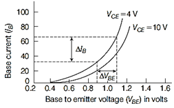 Collector or Output Characteristics A graphical relation between the collector-emitter voltage\[{{V}_{CE}}\] and collector current \[{{I}_{C}}\] by keeping base current \[{{I}_{B}}\] constant is called output characteristics of the transistor. Plot \[{{I}_{C}}\]versus \[{{V}_{CE}}\] graph. Repeat the process for different constant values of \[{{I}_{B}}.\] The output characteristics are as shown,
 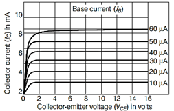 (ii) For the transistor as an amplifier, refer to the (Part-1) sol. 25.


You need to login to perform this action.
You will be redirected in
3 sec

