| Draw the circuit diagram of a common-emitter amplifier using an n-p-n transistor. Draw the input and output waveforms of the signal and also find the expression for its voltage gain. |
| Or |
| Explain with the help of a circuit diagram, the use of p-n junction diode as a half-wave rectifier. Draw a sketch of the input and output waveforms. |
Answer:
Transistor as an amplifier is based on the principle that, a weak input signal given to base region produces an amplified (large) output signal in the collector region. Circuit diagram: 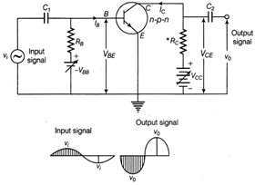 The input voltage \[{{V}_{i}}\] is connected between base and emitter through a capacitor \[{{C}_{1}},\] which blocks DC voltage \[{{V}_{BB}}\] from going towards the AC input source. The output is taken from the collector resistor \[{{R}_{C}}.\] The capacitor \[{{C}_{2}}\] is used to blocks the DC voltage available at the output so that only AC voltage can be obtained at the output. To understand the working of an amplifier let us first assume that input signal voltage \[{{V}_{i}}\] is zero. Then in input loop, we have \[{{V}_{BB}}={{V}_{BE}}+{{I}_{B}}{{R}_{B}}\] ?(i) and in output loop, \[{{V}_{CC}}={{C}_{CE}}+{{I}_{C}}{{R}_{C}}\] ?(ii) Now if signal \[{{V}_{i}}\] is also present, then Eq. (i) is modified as \[{{V}_{BB}}+{{V}_{i}}={{V}_{BE}}+({{I}_{B}}+\Delta {{I}_{B}}){{R}_{B}}\] ?(iii) Subtracting Eq. (i) from Eq. (ii), we get \[{{V}_{i}}=\Delta {{I}_{B}}{{R}_{B}}\Rightarrow \Delta {{I}_{B}}=\frac{{{V}_{i}}}{{{R}_{B}}}\] The change in Ig causes a corresponding change in the collector current \[\Delta {{I}_{C}}\], where\[\Delta {{I}_{C}}={{\beta }_{AC}}\cdot \Delta {{I}_{B}}={{\beta }_{AC}}\frac{{{V}_{i}}}{{{R}_{B}}}\] in the output loop since \[{{V}_{CC}}\] is fixed hence change in \[{{l}_{C}}\] causes a change in \[{{V}_{CE}}\] and Eq. (ii) is modified as \[{{V}_{CC}}=({{V}_{CE}}+{{V}_{C}})+({{I}_{C}}+\Delta {{I}_{C}}){{R}_{C}}\] \[=({{V}_{CE}}+{{V}_{o}})+\left( {{l}_{C}}+{{\beta }_{AC}}\frac{{{V}_{i}}}{{{R}_{B}}} \right){{R}_{C}}\] ?(iv) Subtracting Eq. (ii) from Eq. (iv), we get \[0={{V}_{0}}+{{\beta }_{AC}}.\frac{{{V}_{i}}}{{{R}_{B}}}{{R}_{C}}\] \[\Rightarrow \] Voltage gain \[({{A}_{V}})=\frac{{{V}_{0}}}{{{V}_{i}}}=-{{\beta }_{AC}}\frac{{{R}_{C}}}{{{R}_{B}}}\] The negative sign of \[{{A}_{V}}\] shows that input and output signals differ in phase by \[\pi \] radian that means opposite phase condition. Or Circuit diagram for p-n junction diode as half-wave rectifier is shown in figure below:
 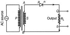 p-n junction diode as a half-wave rectifier Working During first half-cycle of input AC signal, the end A of secondary coil is positive and B is negative therefore p-n junction is forward biased and conduct current in output, resistance \[{{R}_{L}}\] hence output signal is obtained across \[{{R}_{L}}.\]During second half-cycle of input AC signal, the end A of secondary coil is negative and B is positive. Therefore, p-n junction is reverse biased and do not conduct current, hence, there is no output signal across \[{{R}_{L.}}\] Sketch of the input and output waveforms is as shown below.
 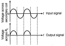 Input/output; waveforms


You need to login to perform this action.
You will be redirected in
3 sec

