
| (i) Give the V-I characteristics of p-n junction diode. |
| (ii) The Zener diode is fabricated by heavily doping of both p and n-sides of junction. Give reason. |
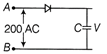
| (iii) A 200 V AC supply is connected between points A and B as shown in the figure. What will be the potential difference V across the capacitor? |
 Or In the figure given below, circuit symbol of a logic gate and two input waveforms A and B are shown.
 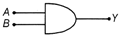 Circuit symbol
 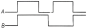 Input waveform
 | (i) Name the logic gate. |
| (ii) Write its truth table. |
| (iii) Give the output waveform. |
Answer:
(i) The \[V-I\] characteristics of p-n junction diode is given below: 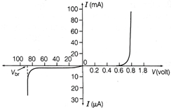 (ii) The both p and n- sides of Zener diode is heavily doped, because due to this depletion region so formed is very thin \[(<{{10}^{-6}}m)\] and the electric field of the junction is extremely high \[(-5\times {{10}^{6}}V/m)\] even for a small reverse bias voltage of about 5 V. (iii) As, p-n junction diode conducts electricity during only half cycle (or forward bias condition). So, potential difference across C = Peak voltage of the given AC voltage, i.e. \[{{V}_{0}}={{V}_{rms}}\times \sqrt{2}=200\times \sqrt{2}=200\sqrt{2}V\] Or (i) AND gate. (ii) Truth table of AND gate is
(iii) Output waveform A B \[Y=A\cdot B\] 0 0 0 0 1 0 1 0 0 1 1 1 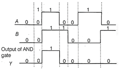






You need to login to perform this action.
You will be redirected in
3 sec