Semiconductor Electronics
Category : Railways
Introduction
On the basis of electrical conductivity\[(\sigma )\]or resistivity \[(\rho =1/\sigma )\] the solids are classified as
(i) Metals - have low resistivity
\[\rho \tilde{\ }{{10}^{-2}}\,to\,{{10}^{-8}}\Omega m\],
\[\sigma \tilde{\ }{{10}^{2}}\,to\,{{10}^{8}}S{{m}^{-1}}\]
(ii) Semiconductors - have intermediate resistivity
\[\rho \tilde{\ }{{10}^{5}}\,to\,{{10}^{0}}\Omega {{m}^{{}}}\]
\[\sigma \tilde{\ }{{10}^{-5}}\,to\,{{10}^{0}}S{{m}^{-1}}\]
(iii) Insulators - have high resistivity
\[\rho \tilde{\ }{{10}^{8}}\Omega {{m}^{{}}}\]
\[\sigma \tilde{\ }{{10}^{-8}}S{{m}^{-1}}\]
i.e. the Semiconductors are the materials whose conductivity is more than insulators but less than conductors.
Intrinsic semiconductors or pure semiconductors in semiconductors forbidden energy gap Eg is more than metals or conductors and less than insulators. Silicon (Si) and Germanium (Ge) are the examples of pure semi-conductors.
In pure or intrinsic semiconductor,
\[{{n}_{e}}={{n}_{h}}={{n}_{i}}\] Where\[{{n}_{e}}=no\].of electrons: \[{{n}_{h}}=no\]. Of holes and\[{{n}_{i}}=no\]. Of intrinsic carrier concentration. Impurity like pentavalent (As, Sb, P) or trivalent (In, B, Al) are added to increase conductivity.
Depending on doping type we have
(a) n- type semiconductor (b) p- type semiconductor
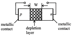
(a) n - type semiconductor: Si or Ge with pentavalent doping. An atom of valency +5 occupies the position of parent atom in crystal lattice. Four valence electrons form 4 covalent bonds but 5th electron is free and weakly bound to parent atom. The ionisation energy (~ 0.01 V for Ge and 0.05V for Si) is small and even at room temperature the electron jumps to conduction band. The dopant is called donor impurity (positively charged).
(b) p - type semiconductor: Si or Ge with trivalent doping means one less electron in the 4 covalent bonds, so the 4th neighbour has a vacancy or hole that can be occupied by an electron from another site. Thus a hole is available for conduction. The trivalent atom is negatively charged as it acquires an electron and is called acceptor atom or impurity.
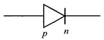
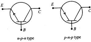
Symbol of p-n junction diode
p-n junction under forward bias: When p-side is connected to positive terminal and n - side to negative terminal of external voltage, it is said to be forward biased.
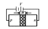
The applied voltage V is opposite to build in Potential\[{{V}_{0}}\], hence depletion layer width decreases and barrier height is reduced to\[({{V}_{0}}-V)\]. There is minority carrier injection, hence charges begin to flow. Current is in the order of mA.
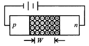
(c) p-n junction under reverse bias: When p-side of p-n junction is connected to -ve terminal and n-side to +ve terminal of the battery, the diode is said to be reverse biased. The direction of applied voltage is same as direction of barrier potential, so barrier height increases to\[({{V}_{0}}+V)\]. This suppresses flow of electrons from \[n\to p\] p and holes from\[p\to n\]. Diffusion current decreases but drift of electrons and holes under the electric field affect remains. This drift current is few\[\mu A\]. The current under reverse bias is independent of applied voltage up to a critical value known as breakdown voltage \[({{V}_{br}})\] when \[V={{V}_{br}}\] diode reverse current increases sharply. If the reverse current is not limited below this, the diode gets destroyed due to overheating.
Zener diode: It is fabricated by heavy doping of p and n sides of p - n junction. Depletion region is thin \[<{{10}^{-6}}m\] . Electric field of junction is high \[\tilde{\ }5\times {{10}^{6}}m\]V/m. Reverse bias ~ 5V.
It is used as voltage regulator.
p-n junction diode is used as a rectifier.
Rectifier is a device which converts A.C. into D.C.
Inverter converts D.C. into A.C.
(a) Photodiode: It is a p - n junction fabricated with a transparent window to allow light photons to fall on it. These photons generate electron hole pairs upon absorption. The generation of electron hole pair is near the junction and due to junction field they remain separated till external load is connected. The electron are collected on n-side and holes on p-side near junction and give rise to an emf. When external load is connected, current flows. The magnitude of current depends on intensity of incident radiation.
(b) Light emitting diode (LED): It consists of heavily doped p - n junction in forward bias. Electrons move from \[n\to p\] and holes from \[p\to n\] (minority carriers). Thus, near junction, minority carrier concentration increases (under no bias it is less) and they combine with majority carriers near the junction to release energy in form of photons with energy equal to or less than band gap energy. As forward bias increases, current increases till light intensity reaches maximum.
(i) Input resistance\[=\frac{Change\,\,in\,base-emitter\,\,voltage}{Base\,Current}\]\[\Rightarrow {{r}_{i}}=\frac{\Delta {{V}_{BE}}}{\Delta {{I}_{B}}}\to \] dynamic resistance
(ii) Output resistance, \[{{r}_{0}}={{\left( \frac{\Delta {{V}_{CE}}}{\Delta {{I}_{C}}} \right)}_{{{I}_{B}}}}\]
(iii) Current amplification factor\[(\beta )\].
\[{{\beta }_{ac}}={{\left( \frac{\Delta {{I}_{C}}}{\Delta {{I}_{B}}} \right)}_{{{V}_{CE}}}}\];\[{{\beta }_{dc}}=\frac{{{I}_{C}}}{{{I}_{B}}}\Rightarrow {{\beta }_{ac}}\simeq {{\beta }_{dc}}\]


You need to login to perform this action.
You will be redirected in
3 sec

