question_answer 1)
In an n-type silicon, which of the following statement is true:
A)
done
clear
B)
done
clear
C)
done
clear
D)
done
clear
View Solution play_arrow
question_answer 2)
Carbon, silicon and germanium have four valence electrons each. These are characterised by valence and conduction bands separated by energy band gap respectively equal to \[{{({{E}_{g}})}_{C,}}{{({{E}_{g}})}_{Si}}\] and \[{{({{E}_{g}})}_{Ge}}\] Which of the following statements is true?
A)
done
clear
B)
done
clear
C)
done
clear
D)
done
clear
View Solution play_arrow
question_answer 3)
The conductivity of a semiconductor increases with increase in temperature because
A)
done
clear
B)
done
clear
C)
done
clear
D)
done
clear
View Solution play_arrow
question_answer 4)
Hole is
A)
done
clear
B)
done
clear
C)
done
clear
D)
done
clear
View Solution play_arrow
question_answer 5)
Semiconductors behave like insulators at ____
A)
done
clear
B)
done
clear
C)
done
clear
D)
done
clear
View Solution play_arrow
question_answer 6)
When the conductivity of a semiconductor is due to rupture of its covalent bond only then the semiconductor is called
A)
done
clear
B)
done
clear
C)
done
clear
D)
done
clear
View Solution play_arrow
question_answer 7)
Tetra valent semiconductor is to be doped with __ valent element to achieve ___ type extrinsic semiconductor.
A)
done
clear
B)
done
clear
C)
done
clear
D)
done
clear
View Solution play_arrow
question_answer 8)
In an unbiased p-n junction, holes diffuse from the p-region to n-region because
A)
done
clear
B)
done
clear
C)
done
clear
D)
done
clear
View Solution play_arrow
question_answer 9)
When a forward bias is applied to a p-n junction, it
A)
done
clear
B)
done
clear
C)
done
clear
D)
done
clear
View Solution play_arrow
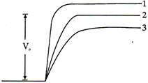
question_answer 10)
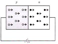
In Figure, \[{{V}_{\operatorname{o}}}\] is the potential barrier across a p-n junction, when no battery is connected across the junction
A)
done
clear
B)
done
clear
C)
done
clear
D)
done
clear
View Solution play_arrow
question_answer 11)
In Figure, assuming the diodes to be ideal,
A)
done
clear
B)
done
clear
C)
done
clear
D)
done
clear
View Solution play_arrow
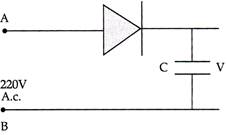
question_answer 12)
A 220 V A.C. supply is connected between points A and B in Figure. What will be the potential difference V across the capacitor?
A)
done
clear
B)
done
clear
C)
done
clear
D)
done
clear
View Solution play_arrow
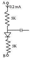
question_answer 13)
The output of the given circuit in Figure
A)
done
clear
B)
done
clear
C)
done
clear
D)
done
clear
View Solution play_arrow
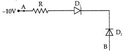
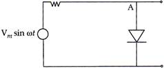
question_answer 14)
In the circuit shown in Figure, if the diode forward voltage drop is 0.3 V, the voltage difference between A and B is
A)
done
clear
B)
done
clear
C)
done
clear
D)
done
clear
View Solution play_arrow
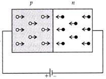
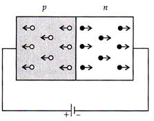
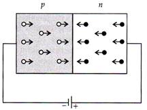
question_answer 15)
Which one of the following diagrams depicts the proper flow or electrons and holes in a forward biased p-n junction diode?
A)
B)
C)
D)
View Solution play_arrow
 done
clear
done
clear
 done
clear
done
clear
 done
clear
done
clear
 done
clear
done
clear