| A | B | Output |
| 0 | 0 | 1 |
| 0 | 1 | 1 |
| 1 | 0 | 1 |
| 1 | 1 | 0 |
Answer:
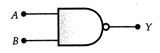
(i) The gate used is NAND gate. Its logic symbol is shown in Fig.
 (ii) When the output of NAND gate is fed to a NOT gate.
Clearly, output \[\Upsilon =A\,.\,B.\] So the new logic gate formed is an AND gate.
Input A
Input B
Output of NAND gate\[\Upsilon '=\overline{\text{A}\text{.B}}\]
Output of NOT gate \[\Upsilon =\overline{\Upsilon }'\].
0
0
1
0
0
1
1
0
1
0
1
0
1
1
0
1


You need to login to perform this action.
You will be redirected in
3 sec

