-
In an n-type silicon, which of the following statement is true :
(a) Electrons are majority carriers and trivalent atoms are the do pants.
(b) Electrons are minority carriers and pentavalent atoms are the do pants.
(c) Holes are minority carriers and pentavalent atoms are the do plants.
(d) Holes are majority carriers and trivalent atoms are the do pants.
View Answer play_arrow
-
Which of the statements given in Exercise is true for p-type semiconductors ?
View Answer play_arrow
-
Carbon, silicon
and germanium have four valence electrons each. These are characterised by
valence and conduction bands separated by energy band gap respectively equal to

and

Which
of the following statements is true ?
(a)

(b)

(c)

(d)

-
In an unbiased p-n junction, holes diffuse from the p-region to w-region because free electrons in the p'region attract them.
(b) they move across the junction by the potential difference.
(c) hole concentration in p-region is more as compared to n-region.
(d) All the above.
View Answer play_arrow
-
When a forward bias is applied to a p-n junction, it
(a) raises the potential barrier
(b) reduces the majority carrier current to zero
(c) lowers the potential barrier
(d) none of the above.
View Answer play_arrow
-
For transistor action, which of the following statements are correct :
(a) Base, emitter and collector regions should have similar size and doping concentrations.
(b) The base region must be very thin and lightly doped.
(c) The emitter junction is forward biased and collector junction is reverse biased.
(d) Both the emitter junction as well as the collector junction are forward biased.
View Answer play_arrow
-
For a transistor amplifier, the voltage gain :
(a) remains constant for all frequencies.
(b) is high at high and low frequencies and constant in the middle frequency range.
(c) is low at high and low frequencies and constant at mid frequencies.
(d) None of the above.
View Answer play_arrow
-
In half-wave rectification, what is the output frequency if the input frequency is 50 Hz. What is the output frequency of a full-wave rectifier for the same input frequency.
View Answer play_arrow
-
For a
CE-transistor amplifier, the audio signal voltage across the collector resistance
of 2

is 2 V. Suppose
the current amplification factor of the transistor is 100, find the input
signal voltage and base current, if the base resistance is 1
.
-
Two amplifiers are connected one after the other in series (cascaded). The first amplifier has a voltage gain of 10 and the second has a voltage gain of 20. If the input signal is 0*01 volt, calculate the output ac signal.
View Answer play_arrow
-
A p-n photodiode is fabricated from a semiconductor with band gap of 2.8 eV.
Can it detect a wavelength of 6000 nm ?
View Answer play_arrow
-
The number of
silicon atoms per m3 is 5 x 1028. This is doped
simultaneously with 5 x 10²² atoms per m3 of Arsenic and
5 x 10²⁰ per m3 atoms of Indium. Calculate the number of
electrons and holes. Given that

Is the material
n- type or p-type ?
-
In an intrinsic
semiconductor the energy gap

is 1.2 eV. Its
hole mobility is much smaller, than electron mobility and independent of
temperature. What is the ratio between conductivity at 600 K and that at 300 K?
Assume that the temperature dependence of intrinsic carrier concentration n, is
given by
Carrier
concentration

is given by
where

is
a constant.
-
in ap-n junction
diode, the current I can be expressed as

where

is
reverse saturation current. V is the voltage across the diode and is positive
for forward bias and negative for reverse bias, and I is the current through
the diode,

is the
Boltzmann constant

and T is the
absolute temperature. If for a given diode

A and T = 300
K, then
(a) What
will be the forward current at forward voltage of 0-6 V ?
(b)
What will be the increase in current if voltage across diode is increased to 0.7
V ?
(c) What
is the dynamic resistance ?
(d) What
will be the current if reverse bias voltage changes from 1 V to 2 V ?
-
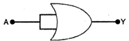
You are given the
two circuits as shown in Figure. Show that circuit (a) acts as OR gate while
the circuit (b) acts as AND gate.
(a)
(b)
-
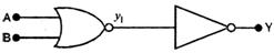
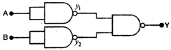
Write the truth
table for a NAND gate connected as given in Fig. Hence identify the exact logic
operation carried out by these circuits.
-
You are given two
circuits as shown in Fig., which consist of NAND gates.
Identify the
logic operation carried out by the two circuits.
(a)
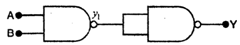
(b)
-
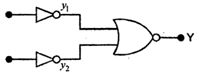
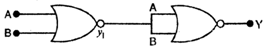
Write the truth
table for circuit given in the Fig. below consisting of NOR gates and identify
the logic operation (OR, AND, NOT) which this circuit is performing.
-
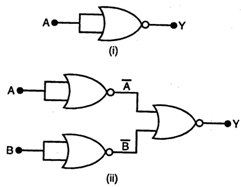
Write the truth
table for the circuits given in the Fig., consisting of NOR gates only.
Identify
the logic operations (OR, AND, NOT) performed by the two circuits.
-
question_answer20)
The conductivity of
a semiconductor increases with increase in temperature because
(a) number
density of free current carriers increases
(b)
relaxation time increases
(c)
both number density of carriers and relaxation time increase
(d)
number density of current carriers increases, relaxation time decreases but
effect of decrease in relaxation time is much less than increase in number
density
View Answer play_arrow
-
question_answer21)
In Fig. 9(EP).1, V0
is the potential barrier across a p-n junction, when no battery is connected
across the junction
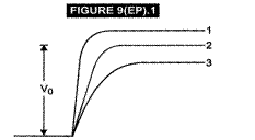 (a)
1 and 3 both correspond to forward bias of junction
(b)
3 corresponds to forward bias of junction and 1 corresponds to reverse bias of
junction (c) 1 corresponds to forward bias and 3 corresponds to reverse bias of
junction
(d)
3 and 1 both correspond to reverse bias of junction
(a)
1 and 3 both correspond to forward bias of junction
(b)
3 corresponds to forward bias of junction and 1 corresponds to reverse bias of
junction (c) 1 corresponds to forward bias and 3 corresponds to reverse bias of
junction
(d)
3 and 1 both correspond to reverse bias of junction
View Answer play_arrow
-
question_answer22)
In Fig. 9(EP).2,
assuming the diodes to be ideal
(a) D1
is forward biased and D2 is reverse biased and hence current flows
from A to B
(b)
D2 is forward biased and D1 is reverse bisaded and hence
no current flows from B to A and vice versa
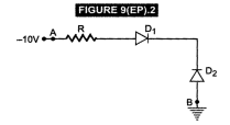 (c) D1 and D2 are both forward biased
and hence current flows from A to B
(d) D1
and D2 are both reverse biased and hence no current flows from A to
B and vice versa
(c) D1 and D2 are both forward biased
and hence current flows from A to B
(d) D1
and D2 are both reverse biased and hence no current flows from A to
B and vice versa
 (a)
220V (b) 110V
(c)
0V (d)
(a)
220V (b) 110V
(c)
0V (d) 
View Answer play_arrow
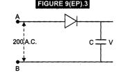
-
question_answer23)
A 220 V A.C. Supply
is connected between points A and B (Fig. 9(EP).3). What will be the potential
difference V across the capacitor?
View Answer play_arrow
-
question_answer24)
Hole is
(a)an
anti-particle of electron
(b)
a vacancy created when an electron leaves a covalent bond
(c)
absence of free electrons
(d)an
artifically created particle
View Answer play_arrow
-
question_answer25)
The output of the
given circuit in Fig. 9(EP).4.
would be zero at all times
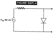 (b)
would be like a half wave rectifier with positive cycles in output
(c)
would be like a half wave rectifier with negative cycles in output
(d)would
be like that of a full wave rectifier
(b)
would be like a half wave rectifier with positive cycles in output
(c)
would be like a half wave rectifier with negative cycles in output
(d)would
be like that of a full wave rectifier
View Answer play_arrow
-
question_answer26)
In the circuit
shown in Fig. 9(EP).5(a), if the diode forward voltage drop is 0.3 V, the voltage
difference between A and B is
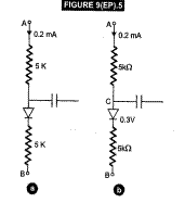 (a)
1.3V (b) 2.3V
(c)
0 (d) 0.5 V
(a)
1.3V (b) 2.3V
(c)
0 (d) 0.5 V
View Answer play_arrow
-
question_answer27)
Truth table for the
given circuit (Fig. 9(EP).6) is
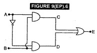 (a)
(a)
|
A
|
B
|
E
|
|
0
|
0
|
1
|
|
0
|
1
|
0
|
|
1
|
0
|
1
|
|
1
|
1
|
0
|
(b)
|
A
|
B
|
E
|
|
0
|
0
|
1
|
|
0
|
1
|
0
|
|
1
|
0
|
0
|
|
1
|
1
|
0
|
(C)
|
A
|
B
|
E
|
|
0
|
0
|
0
|
|
0
|
1
|
1
|
|
1
|
0
|
0
|
|
1
|
1
|
1
|
(d)
|
A
|
B
|
E
|
|
0
|
0
|
0
|
|
0
|
1
|
1
|
|
1
|
0
|
1
|
|
1
|
1
|
0
|
|
|
|
|
View Answer play_arrow
-
question_answer28)
When an electric field
is applied across a semiconductor
(a) electrons
move from lower energy level to higher energy level in the conduction band
(b)
electrons move from higher energy level to lower energy level in the
conduction band
(c)
holes in the valence band move from higher energy level to lower energy level
(d)
holes in the valence band move from lower energy level to higher energy level
View Answer play_arrow
-
question_answer29)
Consider an npn
transitor with its base- emitter junction forward biased and collector base
junction reverse biased. Which of the following statements are true?
(a)Electrons
crossover from emitter to collector
(b)
Holes move from base to collector
(c)
Electrons move from emitter to base
(d)
Electrons from emitter move out of base without going to the collector
View Answer play_arrow
-
question_answer30)
Figure 9(EP).7 shows
that transfer character-istics of a base biased CE transistor. Which of the
following statements are true?
(a) At  =0.4 V, transistor is in active
state
(b)At
= IV, it can be used as an
amplifier
(c)
At = 0.5 V, it can be used as a
switch turned off
(d)
At = 2-5 V, can be used as a
switch turned on
=0.4 V, transistor is in active
state
(b)At
= IV, it can be used as an
amplifier
(c)
At = 0.5 V, it can be used as a
switch turned off
(d)
At = 2-5 V, can be used as a
switch turned on
View Answer play_arrow
-
question_answer31)
In a npn transistor
circuit, the collector current is 10 mA. If 95 per cent of the electrons
emitted reach the collector, which of the following statements are true ?
(a)The
emitter current will be 8 mA
(b)The
emitter current will be 10.53 mA
(c)The
base current will be 0.53 mA
(d)The
base current will be 2 mA
View Answer play_arrow
-
question_answer32)
In the depletion
region of a diode
(a) there
are no mobile charges
(b)
equal number of holes and electrons exist,
(c)
making the region neutral recombination of holes and electrons has taken place
(d)
immobile charged ions exist
View Answer play_arrow
-
question_answer33)
What happens during
regulation action of a Zener diode?
(a) The
current in and voltage across the Zener remains fixed
(b)The
current through the series Resistance (Rs) changes
(c)
The Zener resistance is constant
(d)The
resistance offered by the Zener changes
View Answer play_arrow
-
question_answer34)
To reduce the
ripples in rectifier circuit with capacitor filter
(a) RL
should be increased
(b)
input frequency should be decreased
(c)
input frequency should be increased
(d)
capacitors with high capacitance should be used
View Answer play_arrow
-
question_answer35)
The breakdown in a
reverse biased p-n junction is more likely to occur due to
(a) large
velocity of the minority charge carriers if the doping concentration is small
(b)
large velocity of the minority charge carriers if me doping concentration is
large
(c)
strong electric field in a depletion region if the doping concentration is
small
(d)
strong electric field in the depletion region if the doping concentration is
large
View Answer play_arrow
-
question_answer36)
Why are elemental
dopants for Silicon or Germanium usually chosen from group  or group XV?
View Answer play_arrow
-
question_answer37)
Sn, C and Si, Ge
are all group XIV elements. Yet, 5n is a conductor, C is an insulator while Si
and Ge are semiconductors. Why?
View Answer play_arrow
-
question_answer38)
Can the potential
barrier across a p-n junction be measured by simply connecting a voltmeter
across the junction?
View Answer play_arrow
-
question_answer39)
Draw the output
waveform across the resistor (Fig. 9(EP).8(a)).
View Answer play_arrow
-
question_answer40)
The amplifiers X, Y
and Z are connected in series. If the voltage gains of X, Y and Z are 10,20 and
30, respectively and the input signal is 1 mV peak value, then what is the output
signal voltage (peak value)
(i) if
dc supply voltage is 10 V ?
(ii) if dc
supply voltage is 5 V ?
View Answer play_arrow
-
question_answer41)
In a CE transistor
amplifier there is a current and voltage gain associated with the circuit. In
other words there is a power gain. Considering power a measure of energy, does
the circuit violate conservation of energy?
View Answer play_arrow
-
question_answer42)
(i) Name the type
of a diode whose characteristics are shown in Fig. 9(EP).9(a) and Fig.
9(EP).9(b).
(i) What
does the point P in Fig. (a) represent?
(iii)
What does the points P and Q in Fig. (b) represent ?
View Answer play_arrow
-
question_answer43)
Three photo diodes
D1, D2 and D3 are made of semiconductors
having band gaps of 2.5 eV, 2 eV and 3 eV, respectively. Which ones will be
able to detect light of wavelength 6000  ?
?
View Answer play_arrow
-
question_answer44)
If the resistance R1
is increased Fig. 9(EP).10 (a), how will the readings of the ammeter nd
voltmeter chang?
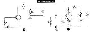
View Answer play_arrow
-
question_answer45)
Two car garages
have a common gate which needs to open automatically when a car enters either
of the garages or cars enter both. Devise a circuit that resembles this
situation using diodes for this situation.
View Answer play_arrow
-
question_answer46)
How would you set
up a circuit to obtain NOT gate using a transistor?
View Answer play_arrow
-
question_answer47)
Explain why
elemental semiconductor can not be used to make visible LEDs.
View Answer play_arrow
-
question_answer48)
Write the truth
table for the circuit shown in Fig. 9(EP).12(a). Name the gate that the circuit
resembles.
View Answer play_arrow
-
question_answer49)
A Zener of power
rating 1 W is to be used as a voltage regulator. If zener has a breakdown of 5
V and it has to regulate voltage which fluctuated between 3 V and 7 V, what should
be the value of Rs for safe operation (Fig. 9(EP).13)?
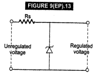
View Answer play_arrow
-
question_answer50)
If each diode in
Fig. 9(EP).14 has a forward bias resistance of 25  and infinite resistance in
reverse bias, what will be the values of the current I
and infinite resistance in
reverse bias, what will be the values of the current I  and
and  ?
?
View Answer play_arrow
-
question_answer51)
In the circuit
shown in Fig. 9(EP).15, when the input voltage of the base resistance is 10 V  is zero and
  is also zero. Find the
values of I b l c and
is also zero. Find the
values of I b l c and  .
.
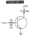
View Answer play_arrow
-
question_answer52)
Draw the output
signals C1 and C2 in the given combination of gates (Fig.
9(EP).16).
View Answer play_arrow
-
question_answer53)
Consider the circuit
arrangement shown in Fig. 9(EP).17(a) for studying input and output characteristics
of npn transistor in CE configuration. Select the values of RB and RC
for a transistor whose VBE = 0.7 V, so that the transistor is
operating at point Q as shown in the characteristics shown in Fig. 9(EP).17(b).
Given that the input impedance of the transistor is very
small and  also find the voltage gain and
power gain of circuit making appropriate assumptions.
also find the voltage gain and
power gain of circuit making appropriate assumptions.
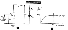
View Answer play_arrow
-
question_answer54)
Assuming the ideal
diode, draw the output waveform for the circuit given in Fig. 9(EP).18(a).
Explain the waveform.
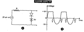
View Answer play_arrow
-
question_answer55)
Suppose a 'n'-type
wafer is created by doping Si crystal having 5 x 1028 atoms/m3
with 1 ppm concentration of As. On the surface 200 ppm Boron is added to create
'P? region in this wafer. Considering  (i)
Calculate the densities of the charge carriers in the n & p regions. (ii)
Comment which charge carriers would contribute largely for the reverse
saturation current when diode is reverse biased.
(i)
Calculate the densities of the charge carriers in the n & p regions. (ii)
Comment which charge carriers would contribute largely for the reverse
saturation current when diode is reverse biased.
View Answer play_arrow
-
question_answer56)
X-OR gate has
following truth table : It is represented by following logic relation
 Build this gate using AND, OR and NOT gates.
|
A
|
B
|
Y
|
|
0
|
0
|
0
|
|
0
|
1
|
1
|
|
1
|
0
|
1
|
|
1
|
1
|
0
|
View Answer play_arrow
-
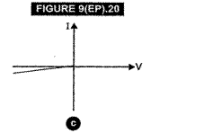
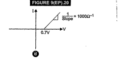
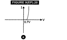
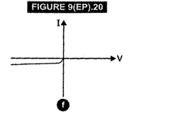
question_answer57)
Consider a box with three terminals on top of it as shown in Fig.
9(EP).20 (a): 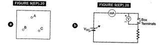 Three components namely, two germanium diodes and one
resistor are connected across these three terminals in some arrangement. A
student performs an experiment in which any two of these three terminals are
connected in the circuit shown in Fig. 9(EP),20 (b). The student obtains graphs
of current-voltage characteristics for unknown combination of components between
the two terminals connected in the circuit. The graphs are
(i) When Aa si positive and B is negative
Three components namely, two germanium diodes and one
resistor are connected across these three terminals in some arrangement. A
student performs an experiment in which any two of these three terminals are
connected in the circuit shown in Fig. 9(EP),20 (b). The student obtains graphs
of current-voltage characteristics for unknown combination of components between
the two terminals connected in the circuit. The graphs are
(i) When Aa si positive and B is negative
 (ii) When A is
negative and B is positive
(ii) When A is
negative and B is positive
 (iii) When B is negative and C is positive
 (iv) When B is
positive and C is negative
(iv) When B is
positive and C is negative
 (v) When A is positive
and C is negative
(v) When A is positive
and C is negative
 (vi) When A is
negative and C is positive
(vi) When A is
negative and C is positive
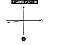
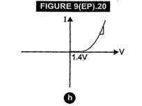 From these graphs of current - voltage characteristic
shown in Fig. 9(EP).20 (c) to (h), determine the arrangement of components
between A, B and C.
From these graphs of current - voltage characteristic
shown in Fig. 9(EP).20 (c) to (h), determine the arrangement of components
between A, B and C.
View Answer play_arrow
-
question_answer58)
For the transistor
circuit shown in Fig. 9(EP).21(a), evaluate VE, RB, RE
given  =
=  ,
,  and VCC=12 V=100.
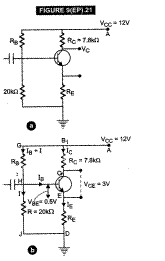
View Answer play_arrow
-
question_answer59)
In the circuit in Fig.
9 (Ep).22 (a), find the value of RC
View Answer play_arrow