(1) In Boolean algebra only two states of variables (0 and 1) are allowed.
(2) The variables (A, B, C ....) of Boolean Algebra are subjected to three operations.
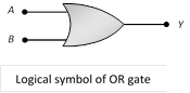
(i) OR Operation : Represented by (+) sign
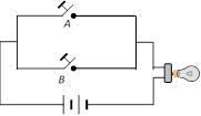
Boolean expression \[Y=A+B\]
When switch A or B is closed ? Bulb glows
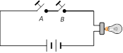
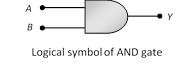
(ii) AND Operation : Represented by \[(.)\] sign
Boolean expression \[Y=A\cdot B\]
When switches A and B both are closed ? Bulb glows
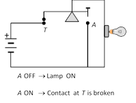
(iii) NOT Operation : Represented by bar over the variables
Boolean expression \[Y=\bar{A}\]
(3) Basic Boolean postulates and laws
(i) Boolean Postulates : \[0+A=A,\] \[1\,\,\cdot \text{ }A=A,\]
\[1+A=1,\]
\[0\cdot A=0,\]
\[A+\bar{A}=1\]
(ii) Identity law : \[A+A=A,\] \[A\cdot A=A\]
(iii) Negation law : \[\overline{{\bar{A}}}=A\]
(iv) Commutative law : \[A+B=B+A,\] \[A\cdot B=B\cdot A\]
(v) Associative law : \[(A+B)+C=A+(B+C),\]
\[(A\cdot B)\cdot C=A\cdot (B\cdot C)\]
(vi) Distributive law : \[A\cdot (B+C)=A\cdot B+A\cdot C\]
\[(A+B)\cdot (A+C)=A+BC\]
(vii) Absorption laws : \[A+A\cdot B=A,\] \[A\cdot (A+B)=A\]
\[\overline{A}\,\text{ }\!\!\cdot\!\!\text{ }\,(A+B\text{)}=\overline{A}\,\text{ }\!\!\cdot\!\!\text{ }\,B\]
(viii) Boolean identities : \[A+\overline{A}\,B=A+B\], \[A(\overline{A}+B)=AB\],
\[A+BC=(A+B)\,(A+C)\], \[(\overline{A}+B)\,\text{ }\!\!\cdot\!\!\text{ }\,\text{(}A+C)\,=\overline{A}C+AB\]
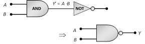
(ix) De Morgan's theorem : It states that the complement of the whole sum is equal to the product of individual complements and vice versa i.e.
\[\overline{A+B}=\bar{A}\cdot \bar{B}\] and \[\overline{A\cdot B}=\bar{A}+\bar{B}\]
 Boolean expression and truth table : \[Y=\overline{A\cdot B}\]


 (3) Realization of NOT gate : The transistor is so biased that the collector voltage \[{{V}_{cc}}=V\] (Voltage corresponding to 1 state) The resistors R and \[{{R}_{1}}\] are so chosen that if the input is low i.e. O, the transistor is in the cut off and hence the voltage appearing at the output will be the same as applied V. Hence Y = V (or state 1) If the input is high, the transistor current is in saturation and the net voltage at the output Y is 0 (in state 0)
 (4) Truth table for NOT gate :
 (3) Realization of AND gate
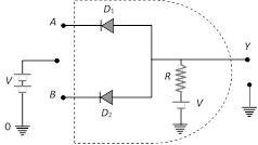 (i) \[A=0,\,\,B=0\] The voltage supply through R is forward biasing diodes \[{{D}_{1}}\] and \[{{D}_{2}}\] (offers low resistance) the voltage V would drop across R The output voltage at Y = the voltage across diode = 0
(ii) A = 0, B = 1 \[{{D}_{1}}=\] conducts, \[{{D}_{2}}=\]Not Conducts the out voltage at Y= The voltage across the diode \[({{D}_{1}})=0\]
(iii) A = 1, B = 0 \[{{D}_{1}}=\]Conducts, \[{{D}_{2}}=\]Not conducts the out voltage at Y= The voltage across the diode \[({{D}_{2}})=0\]
(iv) A = 1, B = 1 None of the diode conducts the out voltage at Y= Battery voltage =1 (4) Truth table for 'AND' gate
(i) \[A=0,\,\,B=0\] The voltage supply through R is forward biasing diodes \[{{D}_{1}}\] and \[{{D}_{2}}\] (offers low resistance) the voltage V would drop across R The output voltage at Y = the voltage across diode = 0
(ii) A = 0, B = 1 \[{{D}_{1}}=\] conducts, \[{{D}_{2}}=\]Not Conducts the out voltage at Y= The voltage across the diode \[({{D}_{1}})=0\]
(iii) A = 1, B = 0 \[{{D}_{1}}=\]Conducts, \[{{D}_{2}}=\]Not conducts the out voltage at Y= The voltage across the diode \[({{D}_{2}})=0\]
(iv) A = 1, B = 1 None of the diode conducts the out voltage at Y= Battery voltage =1 (4) Truth table for 'AND' gate
 (3) Realization of OR gate
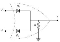 (i) \[A=0,\,\,B=0\] Both diodes \[{{D}_{1}}\] and \[{{D}_{2}}\] do not conduct and hence \[Y=0\]
(ii) \[A=0,\,B=1\] \[{{D}_{1}}=\] Does not conducts, \[{{D}_{2}}=\]Conducts, hence \[Y=1\]
(iii) \[A=1,\,B=0\] \[{{D}_{1}}=\] Conducts, \[{{D}_{2}}=\]
Does not conduct, hence \[Y=1\] (iv) \[A=1,\,B=1\] Both \[{{D}_{1}}\] and \[{{D}_{2}}\] conducts, hence \[Y=1\] (4) Truth table for 'OR' gate
(i) \[A=0,\,\,B=0\] Both diodes \[{{D}_{1}}\] and \[{{D}_{2}}\] do not conduct and hence \[Y=0\]
(ii) \[A=0,\,B=1\] \[{{D}_{1}}=\] Does not conducts, \[{{D}_{2}}=\]Conducts, hence \[Y=1\]
(iii) \[A=1,\,B=0\] \[{{D}_{1}}=\] Conducts, \[{{D}_{2}}=\]
Does not conduct, hence \[Y=1\] (iv) \[A=1,\,B=1\] Both \[{{D}_{1}}\] and \[{{D}_{2}}\] conducts, hence \[Y=1\] (4) Truth table for 'OR' gate
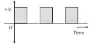
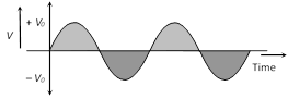 (2) Digital voltage signal : The signal which has only two values. i.e. either a constant high value of voltage or zero value is called digital voltage signal
 e.g. \[=1000+900+70+1\] \[=1\times {{10}^{3}}+9\times {{10}^{2}}+7\times {{10}^{1}}+1\times {{10}^{0}}\]
LSD = Least significant digit
MSD = Most significant digit
(2) Binary number system : A number system which has only two digits i.e. 0 (Low) and 1 (High) is known as binary system. The base of binary number system is 2.
(i) Each digit in binary system is known as a bit and a group of bits is known as a byte.
(ii) The electrical circuit which operates only in these two state i.e. 1 (On or High) and 0 (i.e. Off or Low) are known as digital circuits.
Different names for the digital signals
e.g. \[=1000+900+70+1\] \[=1\times {{10}^{3}}+9\times {{10}^{2}}+7\times {{10}^{1}}+1\times {{10}^{0}}\]
LSD = Least significant digit
MSD = Most significant digit
(2) Binary number system : A number system which has only two digits i.e. 0 (Low) and 1 (High) is known as binary system. The base of binary number system is 2.
(i) Each digit in binary system is known as a bit and a group of bits is known as a byte.
(ii) The electrical circuit which operates only in these two state i.e. 1 (On or High) and 0 (i.e. Off or Low) are known as digital circuits.
Different names for the digital signals


