 (5) A basic common-emitter NPN oscillator is shown in the figure.
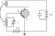 A tank circuit (L-C circuit) is connected in the base-emitter circuit, in which the capacitance C is kept variable. By changing C oscillations of a desired frequency can be obtained. An inductance coil L' connected in the collector-emitter circuit is coupled to coil L.
On completion of the circuit electrical oscillations are developed in the tank circuit. The circuit amplifies these oscillations. A part of the amplifies signal in the collector circuit is fed back in the base circuit by the coupling between L and L'. Due to this feed back amplitude of oscillation builds up till power dissipation in the oscillatory circuit becomes equal to power fed-back. In this state the amplitude of oscillations becomes constant. The oscillations can be transferred to an external circuit by mutual induction in a coil connected in that circuit.
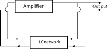
(6) Need for positive feedback : The oscillations are damped due to the presence of some inherent electrical resistance in the circuit. Consequently, the amplitude of oscillations decreases rapidly and the oscillations ultimately stop. Such oscillations are of little practical importance. In order to obtain oscillations of constant amplitude, we make an arrangement for regenerative or positive feedback from the output circuit to the input circuit so that the losses in the circuit can be compensated.
A tank circuit (L-C circuit) is connected in the base-emitter circuit, in which the capacitance C is kept variable. By changing C oscillations of a desired frequency can be obtained. An inductance coil L' connected in the collector-emitter circuit is coupled to coil L.
On completion of the circuit electrical oscillations are developed in the tank circuit. The circuit amplifies these oscillations. A part of the amplifies signal in the collector circuit is fed back in the base circuit by the coupling between L and L'. Due to this feed back amplitude of oscillation builds up till power dissipation in the oscillatory circuit becomes equal to power fed-back. In this state the amplitude of oscillations becomes constant. The oscillations can be transferred to an external circuit by mutual induction in a coil connected in that circuit.
(6) Need for positive feedback : The oscillations are damped due to the presence of some inherent electrical resistance in the circuit. Consequently, the amplitude of oscillations decreases rapidly and the oscillations ultimately stop. Such oscillations are of little practical importance. In order to obtain oscillations of constant amplitude, we make an arrangement for regenerative or positive feedback from the output circuit to the input circuit so that the losses in the circuit can be compensated.
 Comparison between CB, CE and CC amplifier
| Characteristic | Amplifier | |||||||||||||||
| more...
(1) Transistor as CB amplifier
(i) ac current gain \[{{\alpha }_{ac}}=\frac{\text{Small change in collector current (}\Delta {{i}_{c}})}{\text{Small change in collector current (}\Delta {{i}_{e}})}\] \[{{V}_{B}}\] (constant)
(ii) dc current gain \[{{\alpha }_{dc}}\text{(or}\alpha \text{)}=\frac{\text{Collector current(}{{i}_{c}}\text{)}}{\text{Emitter current (}{{i}_{e}})}\] valve of \[{{\alpha }_{dc}}\] lies between 0.95 to 0.99
(iii) Voltage gain \[{{A}_{v}}=\frac{\text{Change in output voltage(}\Delta {{V}_{o}})}{\text{Change in input voltage (}\Delta {{V}_{i}})}\] \[\Rightarrow \] \[{{A}_{v}}={{\alpha }_{ac}}\times \] Resistance gain
(iv) \[\text{Power gain}=\frac{\text{Change in output power(}\Delta {{P}_{o}})}{\text{Change in input power(}\Delta {{P}_{c}})}\] \[\Rightarrow \text{Power gain}=\alpha _{\text{ac}}^{\text{2}}\times \text{Resistance gain}\]
(2) Transistor as CE amplifier
(i) ac current gain \[{{\beta }_{ac}}=\left( \frac{\Delta {{i}_{c}}}{\Delta {{i}_{b}}} \right)\,\]\[{{V}_{CE}}=\]constant
(ii) dc current gain \[{{\beta }_{dc}}=\frac{{{i}_{c}}}{{{i}_{b}}}\]
(iii) Voltage gain : \[{{A}_{v}}=\frac{\Delta {{V}_{o}}}{\Delta {{V}_{i}}}={{\beta }_{ac}}\times \text{Resistance gain}\]
(iv) \[\text{Power gain}=\frac{\Delta {{\text{P}}_{\text{o}}}}{\Delta {{\text{P}}_{\text{i}}}}=\beta _{ac}^{2}\times \text{Resistance gain}\]
(v) Trans conductance \[({{q}_{m}})\] : The ratio of the change in collector current to the change in emitter base voltage is called trans conductance. i.e. \[{{g}_{m}}=\frac{\Delta {{i}_{c}}}{\Delta {{V}_{EB}}}\].
Also\[{{g}_{m}}=\frac{{{A}_{V}}}{{{R}_{L}}}\]; \[{{R}_{L}}=\] Load resistance
(3) Relation between \[\alpha \]and \[\beta \] : \[\beta =\frac{\alpha }{1-\alpha }\] or \[\alpha =\frac{\beta }{1+\beta }\]
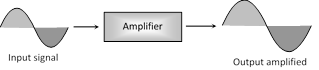
A device which increases the amplitude of the input signal is called amplifier.
 The transistor can be used as an amplifier in the following three configuration
(i) CB amplifier
(ii) CE amplifier
(iii) CC amplifier
(1) NPN transistor as CB amplifier
The transistor can be used as an amplifier in the following three configuration
(i) CB amplifier
(ii) CE amplifier
(iii) CC amplifier
(1) NPN transistor as CB amplifier
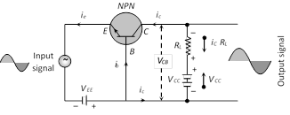 (i) \[{{i}_{e}}={{i}_{b}}+{{i}_{C}};\] \[{{i}_{b}}=5%\] of \[{{i}_{e}}\] and \[{{i}_{C}}=\text{ }95%\] of \[{{i}_{e}}\]
(ii) \[{{V}_{EE}}<{{V}_{CC}}\]
(iii) Net collector voltage \[{{V}_{CB}}={{V}_{CC}}-{{i}_{C}}{{R}_{l}}\]
When the input signal (signal to be amplified) is fed to the emitter base circuit, it will change the emitter voltage and hence emitter current. This in turn will change the collector current \[({{i}_{c}})\]. This will vary the collector voltage \[{{V}_{CB}}\]. This variation of \[{{V}_{CB}}\] will appear as an amplified output. (iv) Input and output signals are in same phase
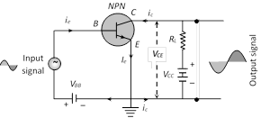
(2) NPN transistor as CE amplifier
(i) \[{{i}_{e}}={{i}_{b}}+{{i}_{C}};\] \[{{i}_{b}}=5%\] of \[{{i}_{e}}\] and \[{{i}_{C}}=\text{ }95%\] of \[{{i}_{e}}\]
(ii) \[{{V}_{EE}}<{{V}_{CC}}\]
(iii) Net collector voltage \[{{V}_{CB}}={{V}_{CC}}-{{i}_{C}}{{R}_{l}}\]
When the input signal (signal to be amplified) is fed to the emitter base circuit, it will change the emitter voltage and hence emitter current. This in turn will change the collector current \[({{i}_{c}})\]. This will vary the collector voltage \[{{V}_{CB}}\]. This variation of \[{{V}_{CB}}\] will appear as an amplified output. (iv) Input and output signals are in same phase
(2) NPN transistor as CE amplifier
 (i) \[{{i}_{e}}={{i}_{b}}+{{i}_{C}};\] \[{{i}_{b}}=5%\] of \[{{i}_{e}}\] and \[{{i}_{c}}=95%\] of \[{{i}_{e}}\]
(ii) \[{{V}_{CC}}>{{V}_{BB}}\]
(iii) Net collector voltage \[{{V}_{CE}}={{V}_{CC}}-{{i}_{c}}{{R}_{l}}\]
(iv) Input and output signals are \[{{180}^{o}}\] out of phase.
(i) \[{{i}_{e}}={{i}_{b}}+{{i}_{C}};\] \[{{i}_{b}}=5%\] of \[{{i}_{e}}\] and \[{{i}_{c}}=95%\] of \[{{i}_{e}}\]
(ii) \[{{V}_{CC}}>{{V}_{BB}}\]
(iii) Net collector voltage \[{{V}_{CE}}={{V}_{CC}}-{{i}_{c}}{{R}_{l}}\]
(iv) Input and output signals are \[{{180}^{o}}\] out of phase.
The low input impedance of the junction transistor is a handicap in certain applications. In addition, it is difficult to incorporate large numbers of them in an integrated circuit and they consume relatively large amounts of power. The field-effect transistor (FET) lacks these disadvantages and is widely used today although slower in operation than junction transistors.
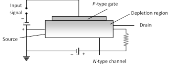 An n-channel FET consists of a block of N-type material with contacts at each end together with a strip of P-type material on one side that is called the gate. When connected as shown, electrons move from the source terminal to the drain terminal through the N-type channel. the PN junction is given a reverse bias, and as a result both the N and P materials near the junction are depleted on charge carriers. The higher the reverse potential on the gate, the larger the depleted region in the channel and the fewer the electrons available to carry the current. Thus the gate voltage controls the channel current. Very little current passes through the gate circuit owing to the reverse bias, and the result is an extremely high input impedance. FET is uni-polar.
A transistor can be connected in a circuit in the following three different configurations. Common base (CB), Common emitter (CE) and Common collector (CC) configuration.
(1) CB configurations : Base is common to both emitter and collector .
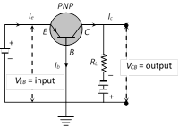 (i) Input current \[={{l}_{e}}\]
(ii) Input voltage \[={{V}_{EB}}\]
(iii) Output voltage \[={{V}_{CB}}\]
(iv) Output current \[={{l}_{C}}\] With small increase in emitter-base voltage \[{{V}_{EB}},\] the emitter current \[{{l}_{e}}\] increases rapidly due to small input resistance.
(v) Input characteristics : If \[{{V}_{CB}}\] constant, curve between \[{{l}_{e}}\] and \[{{V}_{EB}}\] is known as input characteristics. It is also known as emitter characteristics
(i) Input current \[={{l}_{e}}\]
(ii) Input voltage \[={{V}_{EB}}\]
(iii) Output voltage \[={{V}_{CB}}\]
(iv) Output current \[={{l}_{C}}\] With small increase in emitter-base voltage \[{{V}_{EB}},\] the emitter current \[{{l}_{e}}\] increases rapidly due to small input resistance.
(v) Input characteristics : If \[{{V}_{CB}}\] constant, curve between \[{{l}_{e}}\] and \[{{V}_{EB}}\] is known as input characteristics. It is also known as emitter characteristics
 Input characteristics of NPN transistor are also similar to the above figure but \[{{l}_{e}}\] and \[{{V}_{EB}}\] both are negative and \[{{V}_{CB}}\] is positive.
Dynamic input resistance of a transistor is given by
\[{{R}_{i}}={{\left( \frac{\Delta {{V}_{EB}}}{\Delta {{I}_{e}}} \right)}_{{{V}_{CB}}=\,\text{constant}}}\]{\[{{R}_{i}}\] is of the order of \[100\,\Omega \]}
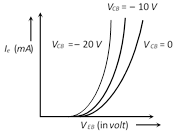
(vi) Output characteristics : Taking the emitter current \[{{i}_{e}}\] constant, the curve drawn between \[{{l}_{C}}\] and \[{{V}_{CB}}\] are known as output characteristics of CB configuration.
Input characteristics of NPN transistor are also similar to the above figure but \[{{l}_{e}}\] and \[{{V}_{EB}}\] both are negative and \[{{V}_{CB}}\] is positive.
Dynamic input resistance of a transistor is given by
\[{{R}_{i}}={{\left( \frac{\Delta {{V}_{EB}}}{\Delta {{I}_{e}}} \right)}_{{{V}_{CB}}=\,\text{constant}}}\]{\[{{R}_{i}}\] is of the order of \[100\,\Omega \]}
(vi) Output characteristics : Taking the emitter current \[{{i}_{e}}\] constant, the curve drawn between \[{{l}_{C}}\] and \[{{V}_{CB}}\] are known as output characteristics of CB configuration.
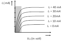 Dynamic output resistance \[{{R}_{o}}={{\left( \frac{\Delta {{V}_{CB}}}{\Delta {{i}_{C}}} \right)}_{{{\text{i}}_{\text{e}}}\text{ }=\text{ constant }}}\]
(2) CE configurations : Emitter is common to both base and collector.
The graphs between voltages and currents when emitter of a transistor is common to input and output circuits are known as CE characteristics of a transistor.
Dynamic output resistance \[{{R}_{o}}={{\left( \frac{\Delta {{V}_{CB}}}{\Delta {{i}_{C}}} \right)}_{{{\text{i}}_{\text{e}}}\text{ }=\text{ constant }}}\]
(2) CE configurations : Emitter is common to both base and collector.
The graphs between voltages and currents when emitter of a transistor is common to input and output circuits are known as CE characteristics of a transistor.
 Input characteristics : Input characteristic curve is drawn between base current \[{{l}_{b}}\] and emitter base voltage \[{{V}_{EB}},\] at constant collector emitter voltage \[{{V}_{CE}}\].
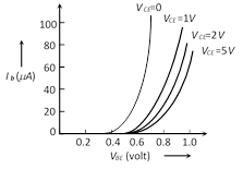 Dynamic input resistance \[{{R}_{i}}={{\left( \frac{\Delta {{V}_{BE}}}{\Delta {{I}_{B}}} \right)}_{{{V}_{CE}}\to \,\text{constant}}}\]
Output characteristics : Variation of collector current \[{{l}_{C}}\] with \[{{V}_{CE}}\] can be noticed for \[{{V}_{CE}}\] between 0 to 1 V only. The value of \[{{V}_{CE}}\] up to which the \[{{l}_{C}}\] changes with \[{{V}_{CE}}\] is called knee voltage. The transistor are operated in the region above knee voltage.
Dynamic input resistance \[{{R}_{i}}={{\left( \frac{\Delta {{V}_{BE}}}{\Delta {{I}_{B}}} \right)}_{{{V}_{CE}}\to \,\text{constant}}}\]
Output characteristics : Variation of collector current \[{{l}_{C}}\] with \[{{V}_{CE}}\] can be noticed for \[{{V}_{CE}}\] between 0 to 1 V only. The value of \[{{V}_{CE}}\] up to which the \[{{l}_{C}}\] changes with \[{{V}_{CE}}\] is called knee voltage. The transistor are operated in the region above knee voltage.
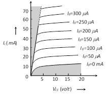 Dynamic output resistance \[{{R}_{0}}={{\left( \frac{\Delta {{V}_{CE}}}{\Delta {{I}_{C}}} \right)}_{{{I}_{B}}\to \,\text{constant}}}\]
(1) There are four possible ways of biasing the two P-N junctions (emitter junction and collector junction) of transistor.
(i) Active mode : Also known as linear mode operation.
(ii) Saturation mode : Maximum collector current flows and transistor acts as a closed switch from collector to emitter terminals.
(iii) Cut-off mode : Denotes operation like an open switch where only leakage current flows.
(iv) Inverse mode : The emitter and collector are inter changed.
Different modes of operation of a transistor
(1) The name of this electronic device is derived from it's fundamental action transfer resistor.
(2) Transistor does not need any heater or hot filament, transistor is small in size and light in weight.
(3) Transistor in general is known as bipolar junction transistor.
(4) Transistor is a current operated device.
(5) It consists of three main regions
(i) Emitter (E) : It provides majority charge carriers by which current flows in the transistor. Therefore the emitter semiconductor is heavily doped.
(ii) Base (B) : The based region is lightly doped and thin.
(iii) Collector (C) : The size of collector region is larger than the two other regions.
(6) Junction transistor are of two types :
(i) NPN transistor : It is formed by sandwiching a thin layer of P-type semiconductor between two N-type semiconductors
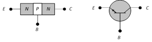 In NPN transistor electrons are majority charge carriers and flow from emitter to base.
(ii) PNP transistor : It is formed by sandwiching a thin layer of N-type semiconductor between two P-type semiconductor
In NPN transistor electrons are majority charge carriers and flow from emitter to base.
(ii) PNP transistor : It is formed by sandwiching a thin layer of N-type semiconductor between two P-type semiconductor
 In PNP transistor holes are majority charge carriers and flow from emitter to base.
In the symbols of both NPN and PNP transistor, arrow indicates the direction of conventional current.
In PNP transistor holes are majority charge carriers and flow from emitter to base.
In the symbols of both NPN and PNP transistor, arrow indicates the direction of conventional current.
Rectifier is a circuit which converts ac to unidirectional pulsating output. In other words it converts ac to dc. It is of following two types
(1) Half wave rectifier : When the P-N junction diode rectifies half of the ac wave, it is called half wave rectifier
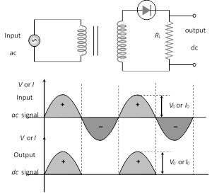 (i) During positive half cycle
Diode \[\xrightarrow{{}}\] forward biased
Output signal \[\xrightarrow{{}}\] obtained
(ii) During negative half cycle
Diode \[\xrightarrow{{}}\] reverse biased
Output signal \[\xrightarrow{{}}\] not obtained
(iii) Output voltage is obtained across the load resistance \[{{R}_{L}}\]. It is not constant but pulsating (mixture of ac and dc) in nature .
(iv) Average output in one cycle
\[{{I}_{dc}}=\frac{{{I}_{0}}}{\pi }\] and \[{{V}_{dc}}=\frac{{{V}_{0}}}{\pi };\,\,{{I}_{0}}=\frac{{{V}_{0}}}{{{r}_{f}}+{{R}_{L}}}\]
(\[{{r}_{f}}=\]forward biased resistance)
(v) r.m.s. output : \[{{I}_{rms}}=\frac{{{I}_{0}}}{2},\,{{V}_{rms}}=\frac{{{V}_{0}}}{2}\]
(vi) The ratio of the effective alternating component of the output voltage or current to the dc component is known as ripple factor.
\[r=\frac{{{I}_{ac}}}{{{I}_{dc}}}={{\left[ {{\left( \frac{{{I}_{rms}}}{{{I}_{dc}}} \right)}^{2}}-1 \right]}^{1/2}}=1.21\]
(vii) Peak inverse voltage (PIV) : The maximum reverse biased voltage that can be applied before commoncement of Zener region is called the PIV. When diode is not conducting PIV across it \[={{V}_{0}}\]
(viii) Efficiency :
(i) During positive half cycle
Diode \[\xrightarrow{{}}\] forward biased
Output signal \[\xrightarrow{{}}\] obtained
(ii) During negative half cycle
Diode \[\xrightarrow{{}}\] reverse biased
Output signal \[\xrightarrow{{}}\] not obtained
(iii) Output voltage is obtained across the load resistance \[{{R}_{L}}\]. It is not constant but pulsating (mixture of ac and dc) in nature .
(iv) Average output in one cycle
\[{{I}_{dc}}=\frac{{{I}_{0}}}{\pi }\] and \[{{V}_{dc}}=\frac{{{V}_{0}}}{\pi };\,\,{{I}_{0}}=\frac{{{V}_{0}}}{{{r}_{f}}+{{R}_{L}}}\]
(\[{{r}_{f}}=\]forward biased resistance)
(v) r.m.s. output : \[{{I}_{rms}}=\frac{{{I}_{0}}}{2},\,{{V}_{rms}}=\frac{{{V}_{0}}}{2}\]
(vi) The ratio of the effective alternating component of the output voltage or current to the dc component is known as ripple factor.
\[r=\frac{{{I}_{ac}}}{{{I}_{dc}}}={{\left[ {{\left( \frac{{{I}_{rms}}}{{{I}_{dc}}} \right)}^{2}}-1 \right]}^{1/2}}=1.21\]
(vii) Peak inverse voltage (PIV) : The maximum reverse biased voltage that can be applied before commoncement of Zener region is called the PIV. When diode is not conducting PIV across it \[={{V}_{0}}\]
(viii) Efficiency :
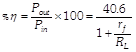 If \[{{R}_{L}}>>{{r}_{f}}\] then \[\eta =40.6%\]
If \[{{R}_{L}}={{r}_{f}}\] then \[\eta =20.3%\]
(ix) Form factor = \[\frac{{{I}_{rms}}}{{{I}_{dc}}}=\frac{\pi }{2}=1.57\]
(x) The ripple frequency \[(\omega )\] for half wave rectifier is same as that of ac.
(2) Full wave rectifier : It rectifies both halves of ac input signal.
If \[{{R}_{L}}>>{{r}_{f}}\] then \[\eta =40.6%\]
If \[{{R}_{L}}={{r}_{f}}\] then \[\eta =20.3%\]
(ix) Form factor = \[\frac{{{I}_{rms}}}{{{I}_{dc}}}=\frac{\pi }{2}=1.57\]
(x) The ripple frequency \[(\omega )\] for half wave rectifier is same as that of ac.
(2) Full wave rectifier : It rectifies both halves of ac input signal.
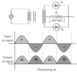 (i) During positive half cycle
Diode : \[{{D}_{1}}\] \[\xrightarrow{\,\,\,\,\,\,\,}\] forward biased
\[{{D}_{2}}\] \[\xrightarrow{\,\,\,\,\,\,\,}\] reverse biased
Output signal \[\xrightarrow{\,\,\,\,\,\,\,}\]obtained due to \[{{D}_{1}}\] only
(ii) During negative half cycle
Diode : \[{{D}_{1}}\] \[\xrightarrow{\,\,\,\,\,\,\,}\] reverse biased
\[{{D}_{2}}\] \[\xrightarrow{\,\,\,\,\,\,\,}\] forward biased
Output signal \[\xrightarrow{\,\,\,\,\,\,\,}\] obtained due to \[{{D}_{2}}\] only
(iii) Fluctuating dc
(i) During positive half cycle
Diode : \[{{D}_{1}}\] \[\xrightarrow{\,\,\,\,\,\,\,}\] forward biased
\[{{D}_{2}}\] \[\xrightarrow{\,\,\,\,\,\,\,}\] reverse biased
Output signal \[\xrightarrow{\,\,\,\,\,\,\,}\]obtained due to \[{{D}_{1}}\] only
(ii) During negative half cycle
Diode : \[{{D}_{1}}\] \[\xrightarrow{\,\,\,\,\,\,\,}\] reverse biased
\[{{D}_{2}}\] \[\xrightarrow{\,\,\,\,\,\,\,}\] forward biased
Output signal \[\xrightarrow{\,\,\,\,\,\,\,}\] obtained due to \[{{D}_{2}}\] only
(iii) Fluctuating dc  for \[{{r}_{ff}}<<{{R}_{L}},\,\,\eta =81.2%\]
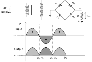
(3) Full wave bridge rectifier : Four diodes \[{{D}_{1}},\,\,{{D}_{2,\,\,}}{{D}_{3}}\] and \[{{D}_{4}}\] are used in the circuit.
During positive half cycle \[{{D}_{1}}\] and \[{{D}_{3}}\] are forward biased and D2 and D4 are reverse biased
During negative half cycle \[{{D}_{2}}\] and \[{{D}_{4}}\] are forward biased and \[{{D}_{1}}\] and \[{{D}_{3}}\] are reverse biased
for \[{{r}_{ff}}<<{{R}_{L}},\,\,\eta =81.2%\]
(3) Full wave bridge rectifier : Four diodes \[{{D}_{1}},\,\,{{D}_{2,\,\,}}{{D}_{3}}\] and \[{{D}_{4}}\] are used in the circuit.
During positive half cycle \[{{D}_{1}}\] and \[{{D}_{3}}\] are forward biased and D2 and D4 are reverse biased
During negative half cycle \[{{D}_{2}}\] and \[{{D}_{4}}\] are forward biased and \[{{D}_{1}}\] and \[{{D}_{3}}\] are reverse biased
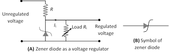
(1) Zener diode : It is a highly doped p-n junction which is not damaged by high reverse current. It can operate continuously, without being damaged in the region of reverse background voltage. In the forward bias, the zener diode acts as ordinary diode. It can be used as voltage regulator
 (2) Light emitting diode (LED) : Specially designed diodes, which give out light radiations when forward biases. LED'S are made of GaAsp, Gap etc. These are forward biased P-N-junctions which emits spontaneous radiation.
Current Affairs CategoriesArchive
Trending Current Affairs


You need to login to perform this action. | ||||||||||||||||